A manufacturing process of a multi-layer circuit board with a large-aperture pad

A technology of multi-layer circuit and manufacturing process, which is applied in the direction of multi-layer circuit manufacturing, printed circuit, printed circuit parts, etc., can solve the problems of personnel injury, energy waste, and take-out danger, etc., so as to reduce the operation process, smelt efficiently, improve efficiency effect

Active Publication Date: 2022-03-29
广德通灵电子有限公司
View PDF0 Cites 0 Cited by
  • Summary
  • Abstract
  • Description
  • Claims
  • Application Information

AI Technical Summary

Problems solved by technology

[0003] During the production and processing of multi-layer circuit boards, it is necessary to manually superimpose the circuit board and the gel layer, and then integrate it into a thin plate with the pressing plate and furnace equipment. The traditional furnace equipment cannot efficiently clean the circuit board and the gel layer. If the integration is carried out, the temperature in the furnace equipment is easy to leak, causing personal injury and energy waste. At the same time, the integrated circuit board and rubber layer are in a high temperature state, and it is dangerous to take them out of the furnace artificially. At the same time, wait for other Natural cooling makes the production and processing of multilayer circuit boards inefficient

Method used


Image

  • A manufacturing process of a multi-layer circuit board with a large-aperture pad
  • A manufacturing process of a multi-layer circuit board with a large-aperture pad
  • A manufacturing process of a multi-layer circuit board with a large-aperture pad

Examples


Embodiment Construction

[0047] The technical solutions of the present invention will be clearly and completely described below in conjunction with the embodiments. Apparently, the described embodiments are only some of the embodiments of the present invention, not all of them. Based on the embodiments of the present invention, all other embodiments obtained by persons of ordinary skill in the art without creative efforts fall within the protection scope of the present invention.

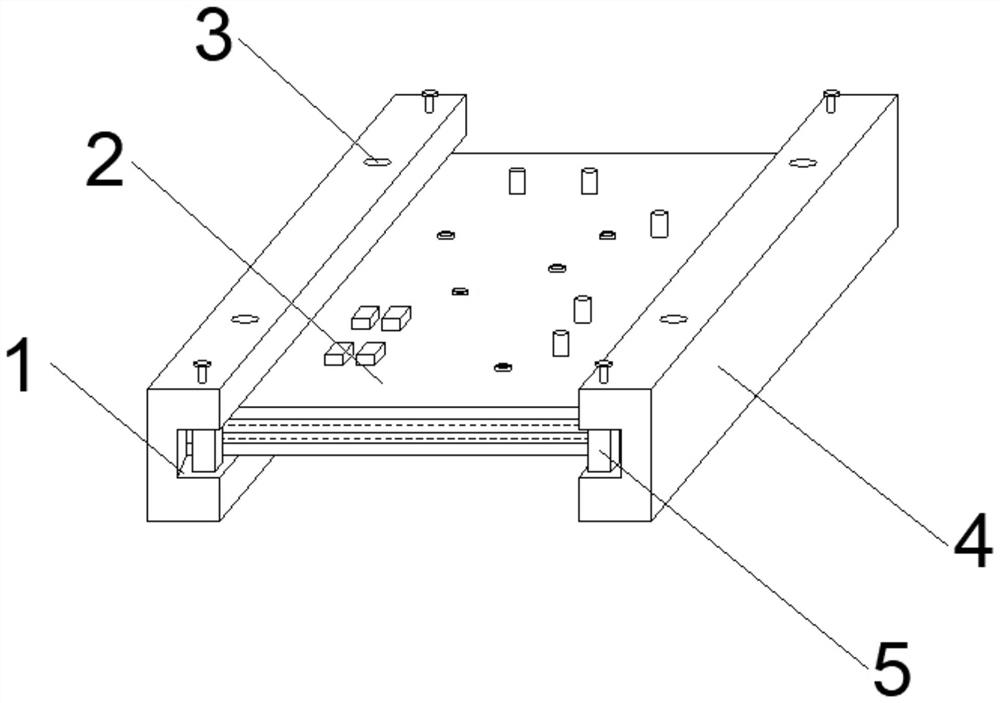
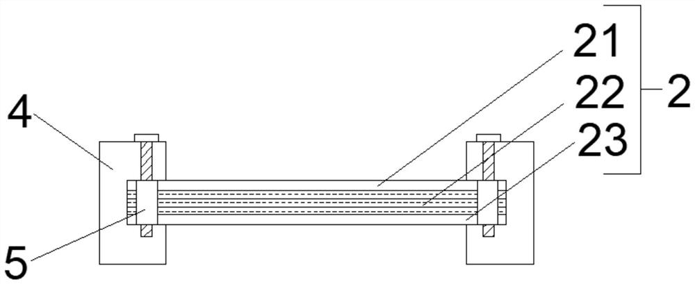
[0048] see Figure 1-7 As shown, a multilayer circuit board with large-aperture pads includes a multilayer circuit board body 2. Both ends of the multilayer circuit board body 2 are provided with protective shells 4, and the protective shells 4 are close to the multilayer circuit board body 2. One side of the multilayer circuit board body 2 is provided with a card slot 1, and the two ends of the multilayer circuit board body 2 are engaged with the corresponding card slot 1, and the four corners of the multilayer circuit boa...


PUM


Abstract

The invention discloses a manufacturing process of a multi-layer circuit board with large-aperture pads. The manufacturing process of a multi-layer circuit board with large-aperture pads comprises the following steps: step 1, first wrapping a copper-plated fiberglass plate A layer of film, and then manually put the copper-coated fiberglass plate wrapped in the film into the corresponding exposure equipment to expose the electronic circuit. The light passes through the template to make the electronic circuit appear on the film, and the exposed film forms a protection on the electronic circuit. Layer; the moving plate is limited by the first limit rod to prevent the deviation of the moving plate during the movement process. The top of the moving plate passes through the first limit hole and is fixedly connected with the left end of the bottom surface of the first transmission plate , by driving the motor to drive the first plate to transport the second plate to the top surface of the second conveying plate, reducing the manual operation of moving the multilayer circuit board into the furnace equipment and reducing the risk of processing.

Description

technical field [0001] The invention relates to the technical field of multilayer circuit boards, in particular to a manufacturing process of multilayer circuit boards with large-aperture pads. Background technique [0002] The market for the circuit board segment continues to evolve, mainly due to two drivers. First, the market space of the circuit board application industry continues to expand, and the application of the communication industry and the notebook computer industry has improved, making the high-end multilayer circuit board market grow very rapidly, and the current application ratio has reached 50%. At the same time, the proportion of digital circuit boards used in color TVs, mobile phones, and automotive electronics has also increased significantly, which has continuously expanded the space for the circuit board industry. [0003] During the production and processing of multi-layer circuit boards, it is necessary to manually superimpose the circuit board and ...

Claims


Application Information

Patent Timeline
Patent Type & Authority Patents(China)
IPC IPC(8): H05K1/02H05K1/11H05K3/46H05K7/20H05K13/00
CPCH05K1/0298H05K1/111H05K3/46H05K7/20136H05K13/0015
Inventor 严浩
Owner 广德通灵电子有限公司
Why Eureka
Try Eureka