Wide voltage input four-tube Buck-Boost circuit
A wide voltage input and circuit technology, which is applied in the direction of converting DC power input to DC power output, electrical components, and adjusting electrical variables, can solve the problems of reverse polarity of output voltage and harsh selection of switch tube withstand voltage, etc., and achieve reduction Cost, drive circuit is stable and simple, and the effect of cost reduction
- Summary
- Abstract
- Description
- Claims
- Application Information
AI Technical Summary
Problems solved by technology
Method used
Image
Examples
no. 1 example
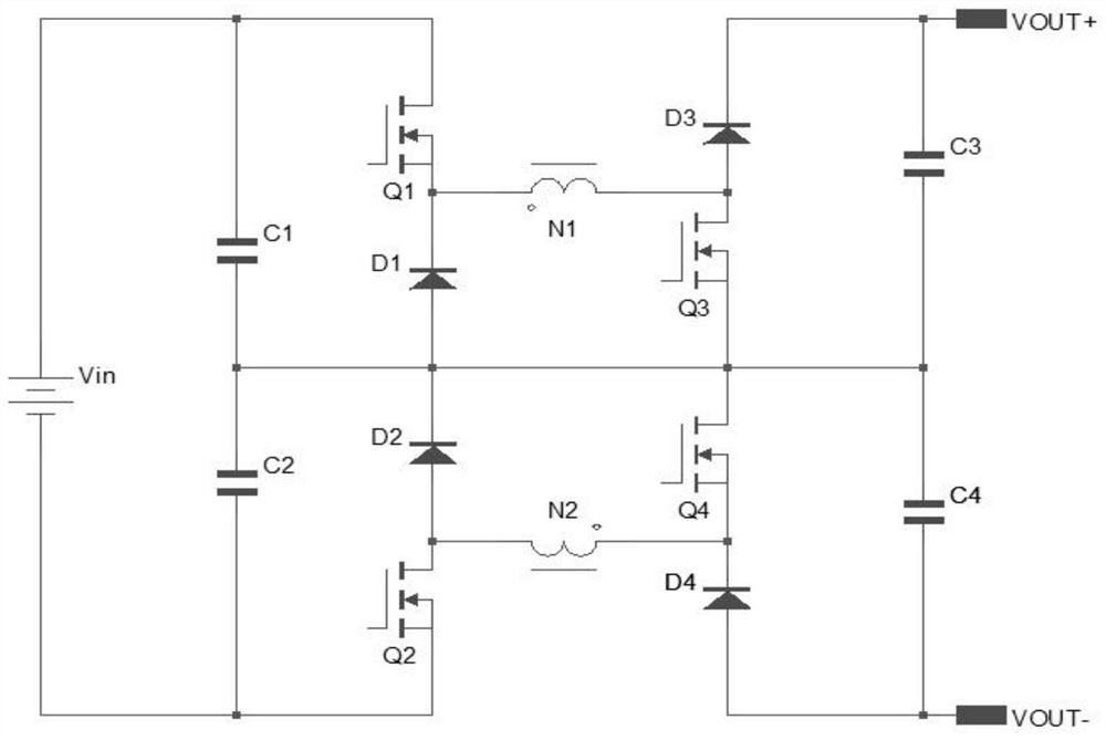
[0023] image 3 It is the schematic diagram of the wide voltage input Buck-Boost circuit of the first embodiment, which includes capacitor C1, capacitor C2, capacitor C3, capacitor C4, switch Q1, switch Q2, switch Q3, switch Q4, diode D1, diode D2 , diode D3, diode D4, coupled inductance and neutral line, wherein the coupled inductance is composed of winding inductance N1 and winding inductance N2;
[0024] Its connection relationship is as follows:
[0025] The anode of the input power supply Vin is connected to the drain of the switch tube Q1, and the source of the switch tube Q1 is connected to the cathode of the diode D1 and the end of the winding inductance N1 of the coupled inductor; the first end of the capacitor C1 is connected to the positive terminal of the input power supply Vin, and the capacitor C1 The second end of the capacitor C2 is connected to the first end of the capacitor C2; the first end of the capacitor C2 is connected to the cathode of the diode D2 and...
no. 2 example
[0029] Such as Figure 4 As shown, it is the schematic diagram of the wide voltage input Buck-Boost circuit of the second embodiment of the present invention. Compared with the first embodiment, the difference lies in that the resistor R1, the resistor R2, the resistor R3, the resistor R4 and the capacitor C5 are added.
[0030] Its connection relationship is as follows:
[0031] The anode of the input power supply Vin is connected to the first end of the capacitor C1, the first end of the resistor R1 and the drain of the switch Q1; the second end of the capacitor C1 is connected to the first end of the capacitor C2; the source of the switch Q1 is connected to the diode D1 The cathode of the winding inductance N1 and the end of the same name; the first end of the capacitor C2, the second end of the resistor R1, the first end of the resistor R2, the cathode of the diode D2 and the anode of the diode D1, the second end of the capacitor C2 is connected to the input power supply ...
no. 3 example
[0034] Such as Figure 5 As shown, it is the schematic diagram of the wide-voltage input Buck-Boost circuit of the third embodiment of the present invention. Compared with the second embodiment, the difference is that the freewheeling diode D1, diode D2, diode D3, and diode D4 are replaced with switches Tube Q5, switch tube Q6, switch tube Q7, switch tube Q8.
[0035] Its connection relationship is as follows:
[0036] The positive pole of the input power supply Vin is connected to the first end of the capacitor C1, the first end of the resistor R1 and the drain of the switch tube Q1; the second end of the capacitor C1 is connected to the first end of the capacitor C2; the source of the switch tube Q1 is connected to the switch tube The drain of Q5 and the end of the same name of the winding inductance N1; the first end of the capacitor C2 is connected to the second end of the resistor R1, the first end of the resistor R2, the source of the switch Q5 and the drain of the swit...
PUM
 Abstract
Description
Claims
Application Information


