Automatic loading, unloading, shaping and installing integrated robot for IGBT chip

An automatic loading and unloading and robot technology, applied in semiconductor/solid-state device manufacturing, conveyor objects, transportation and packaging, etc., can solve problems affecting processing efficiency, chip positioning error, high labor cost, etc., and achieve the effect of solving chip positioning error

Pending Publication Date: 2021-07-20
HANGZHOU WOLEI INTELLIGENT TECH
View PDF0 Cites 4 Cited by
  • Summary
  • Abstract
  • Description
  • Claims
  • Application Information

AI Technical Summary

Problems solved by technology

The chip installation of the traditional IGBT module adopts the method of manual installation, which has low efficiency and high labor cost
[0003] On the other hand, the chip shaping process in the current IGBT chip assembly is generally divided into two processes: the pin cutting process and the pin bending process. Cut the pins to make the pin length of the chip meet the installation requirements; then, move to the equipment of the pin bending process to bend the pins of the chip; the chip shaping process in the current IGBT chip assembly, Due to the need to go through two processing steps successively, it not only affects the processing efficiency, but also is prone to the positioning error of the chip due to the two processing steps, which affects the dimensional accuracy of the chip after cutting and bending.

Method used


Image

  • Automatic loading, unloading, shaping and installing integrated robot for IGBT chip
  • Automatic loading, unloading, shaping and installing integrated robot for IGBT chip
  • Automatic loading, unloading, shaping and installing integrated robot for IGBT chip

Examples


specific Embodiment 1

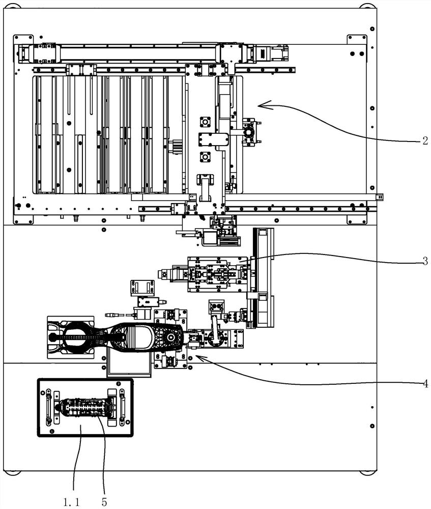
[0085] Specific embodiment one: as figure 1 , figure 2 , image 3As shown, an integrated robot for automatic loading, unloading, shaping and installation of IGBT chips includes a frame, a tray 1.1, an automatic chip unloading machine 2, a chip shaping station 3 and a chip mounting station 4. The tray is used to place the IGBT module 5, and the tray is provided with vertically distributed positioning pins for positioning the IGBT module. The IGBT module is placed on the tray. The IGBT module has a process hole, and the process hole is matched with the positioning pin. In this embodiment, the tray is fixedly placed on the rack.

[0086] The chip automatic blanking machine is used to output the chips in the chip material tube one by one, so as to realize the automatic chip blanking output of the chip material tube; in this embodiment, the chip automatic blanking machine is an automatic chip blanking machine in the prior art .

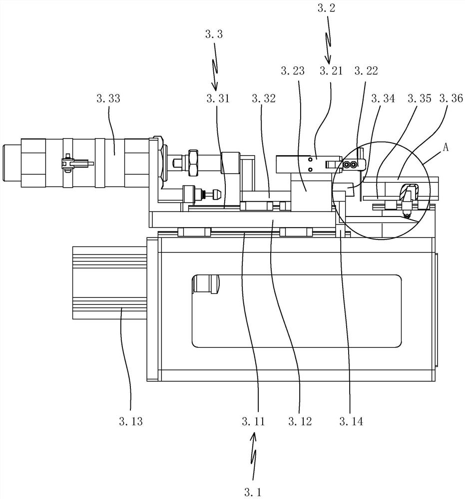
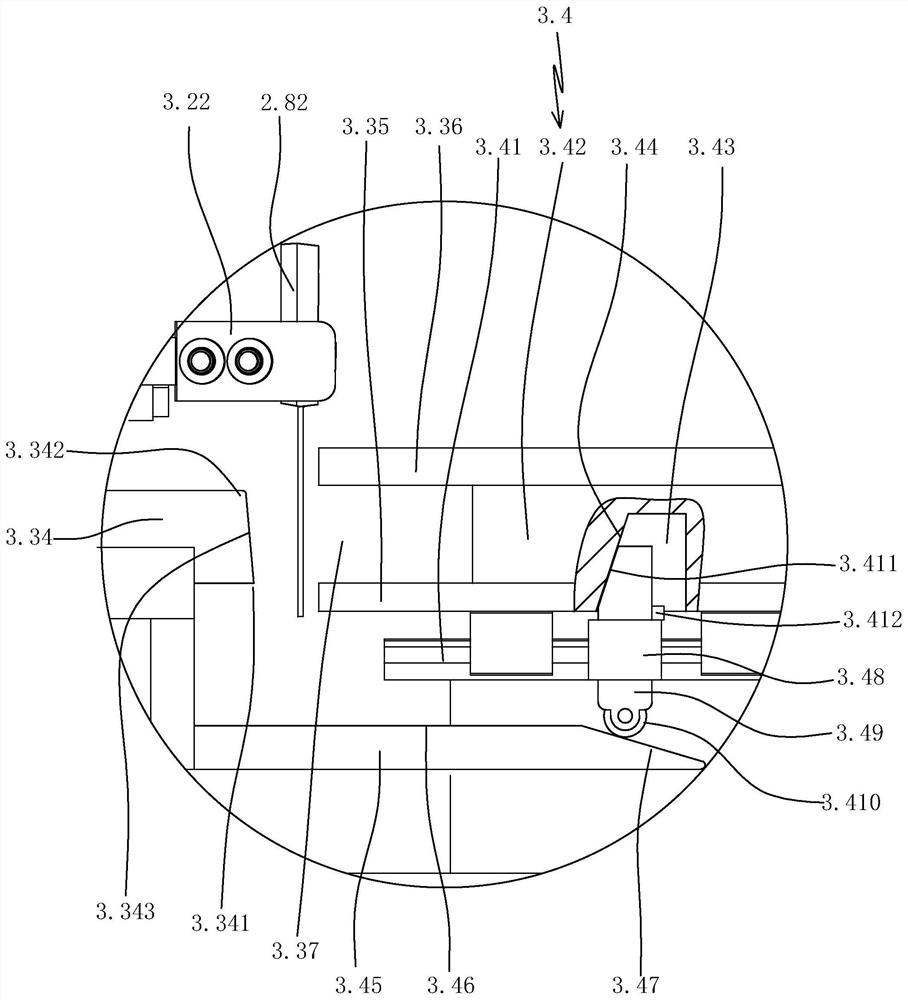
[0087] The chip shaping station includes a chi...

specific Embodiment 2

[0109] Specific embodiment two, all the other structures of this embodiment refer to specific embodiment one, and its difference is:

[0110] Such as Figure 4 As shown, the chip automatic unloading machine includes a first material tube grabbing manipulator 2.2, a second material tube grabbing manipulator 2.4, a chip material warehouse 2.1, a chip material tube direction adjustment device 2.3, a material pushing device 2.5, and a material tube rotating device 2.6 2.7 with chip output device.

[0111] The chip magazine is used to place chip tubes. Such as Figure 5 As shown, the chip material tube 2.8 includes a material tube 2.81 with a rectangular cross section and a number of chips 2.82 sequentially distributed in the material tube. The chip includes a chip body 2.821 and several pins 2.822. The center of gravity of the chip is distributed in the middle of the chip body. The pins of the chips are distributed on the same side of the chip, and the pins of the chips in the...

specific Embodiment 3

[0131] Specific embodiment three, all the other structures of this embodiment refer to specific embodiment three, and its difference is:

[0132] Such as Figure 9 As shown, the chip mounting station of this embodiment includes a loading station 4.3, a detection station 4.4, a blanking station, a rotating platform 4.1 and a platform rotating drive device arranged on the frame, and the platform rotating drive device is used for Drive the rotating platform to rotate. In this embodiment, the platform rotating driving device is a driving motor or a rotating cylinder. The rotary platform is provided with four chip positioning stations 4.2 evenly distributed around the circumference of the rotary axis of the rotary platform. Each chip positioning station includes a chip positioning block 4.21 and a clamping cylinder 4.22 arranged on the upper surface of the rotary platform. The clamping cylinder is used for clamping and positioning the chip placed on the chip positioning block. I...


PUM


Abstract

The invention discloses an automatic loading, unloading, shaping and installing integrated robot for an IGBT chip. The automatic loading, unloading, shaping and mounting integrated robot can realize automatic mounting of the IGBT chip, can effectively solve the problem that the size precision of the chip after pin shearing, bending and forming is affected due to chip positioning errors of two machining procedures of pin shearing and bending. The robot comprises a rack, a tray used for placing an IGBT module; an automatic chip discharging machine used for outputting the chips in the chip material pipe one by one; a chip shaping station comprising a chip pin shearing and bending device, wherein the chip pin shearing and bending device is used for carrying out pin shearing and bending on the pins of the chips so as to realize pin shearing and bending of the pins of the chips; and a chip mounting station used for carrying the chip which passes through the chip shaping station and is subjected to pin cutting and bending of the chip pins to the IGBT module on the tray.

Description

technical field [0001] The invention relates to a chip assembly device, in particular to an integrated robot for automatic loading, unloading, shaping and installing of IGBT chips. Background technique [0002] There are several chips on the current IGBT module, and the chip assembly includes the following steps in turn, the chip blanking process of the chip material tube, the chip material tube is the tube-mounted chip, which is one tube by one tube; currently, chip material tube blanking is generally used The machine outputs the chips in the chip material tube. Specifically, when the chip material tube blanking machine is working, the chip material tube is tilted at a certain angle, and then the chips in the chip material tube are output one by one under the action of gravity; the chip shaping process, IGBT chip The pins of the chip need to be cut and bent according to the installation requirements of the IGBT module, so that the length of the chip pins meets the installat...

Claims


Application Information

Patent Timeline
Patent Type & Authority Applications(China)
IPC IPC(8): H01L21/677
CPCH01L21/67706H01L21/67721H01L21/67742
Inventor 郭斌李静伟薛清风马欣欣田建威胡烨桦王龙
Owner HANGZHOU WOLEI INTELLIGENT TECH
Why Eureka
Try Eureka