A driving timing control method of a cmos detector

A technology for driving timing and control methods, which is applied to color TV parts, TV system parts, TVs, etc. It can solve problems such as blurred images and prone to abnormal working conditions, so as to achieve normal working conditions, improve stability and reliability effect

Active Publication Date: 2022-05-10
CHANGCHUN INST OF OPTICS FINE MECHANICS & PHYSICS CHINESE ACAD OF SCI
View PDF4 Cites 0 Cited by
  • Summary
  • Abstract
  • Description
  • Claims
  • Application Information

AI Technical Summary

Problems solved by technology

[0003] The present invention provides a driving sequence control method for a CMOS detector in order to solve the problem that the existing CMOS detector is prone to abnormal working conditions, resulting in blurred images, etc.

Method used


Image

  • A driving timing control method of a cmos detector
  • A driving timing control method of a cmos detector
  • A driving timing control method of a cmos detector

Examples


Embodiment Construction

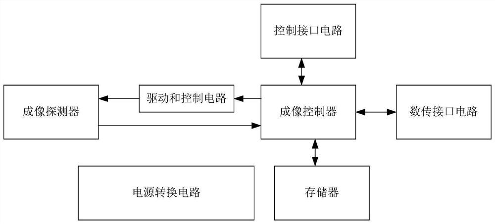
[0020] combine Figure 1 to Figure 5 Describe this implementation mode, a driving sequence control method of a CMOS detector, which is implemented based on a CMOS imaging system, such as figure 1 As shown, the CMOS imaging system mainly includes power conversion circuits, imaging detectors, drive and control circuits, imaging controllers, data transmission interface circuits, memory and control interface circuits. The power conversion circuit provides power supply for each part; the external input control communication signal is sent to the imaging controller through the control interface circuit; the driving and control signal generated by the imaging controller is sent to the imaging detector after passing through the driving and control circuit; The non-uniform correction coefficient is stored in the memory; the digital image data output by the imaging detector is conditioned by the imaging controller and then output through the digital transmission interface circuit.

[0...


PUM


Abstract

A driving timing control method for a CMOS detector, relating to the technical field of CMOS detector imaging control, solving the problems that existing CMOS detectors are prone to abnormal working conditions, resulting in blurred images, etc. The imaging controller includes power-on timing and SPI modules, training module, data conditioning module, drive sequence module, 422 communication and analysis module and data transmission module; the power-on sequence and SPI module are composed of counters and D flip-flops under the same source clock domain; the drive sequence control method of the present invention is based on training The optimal driving timing signal position setting ensures that the internal sampling signal of the detector is in a stable and reliable position, the working state is normal, and it will not appear unstable with the external environment such as temperature changes. The timing reset signal is resampled and output to ensure a relatively constant phase relationship between the timing reset signal and each drive control signal, and to avoid sampling metastable states inside the detector, thereby improving the stability and reliability of the application.

Description

technical field [0001] The invention relates to a driving sequence control method of a CMOS detector, in particular to a driving sequence control method of a CMOS detector applied by inputting a high-frequency differential clock. Background technique [0002] The CMOS detector needs to provide a reference clock from the outside first. In order to avoid the abnormal working state of the phase-locked loop (PLL) and affect the reliability, a high-frequency clock can be directly input. In order to control the working mode of the detector, the content of the internal SPI register is usually configured. In order to save configuration time, the SPI reading and writing frequency is usually set higher; in order to realize the normal operation of the detector, it is necessary to input multiple A driving and control signal; in addition, in the power-on and reset stages of the detector, it is also necessary to output a power-on reset signal and a timing reset signal. If the transition ...

Claims


Application Information

Patent Timeline
Patent Type & Authority Patents(China)
IPC IPC(8): H04N5/374
CPCH04N25/76
Inventor 余达韩诚山薛栋林姜肖楠张博研张艳鹏李俊霖
Owner CHANGCHUN INST OF OPTICS FINE MECHANICS & PHYSICS CHINESE ACAD OF SCI
Why Eureka
Try Eureka