Void free low stress fill
A technology for substrate and metal deposition, which can be used in semiconductor/solid-state device parts, coatings, gaseous chemical plating, etc., and can solve problems such as no voids and low stress
- Summary
- Abstract
- Description
- Claims
- Application Information
AI Technical Summary
Problems solved by technology
Method used
Image

Examples
Embodiment Construction
[0017] In the following description, numerous specific details are set forth in order to provide a thorough understanding of the present invention. The present invention may be practiced without some or all of these specific details. In other instances, well known process operations have not been described in detail in order not to unnecessarily obscure the present invention. While the invention will be described in conjunction with specific embodiments, it will be understood that it is not intended to limit the invention to these implementations.
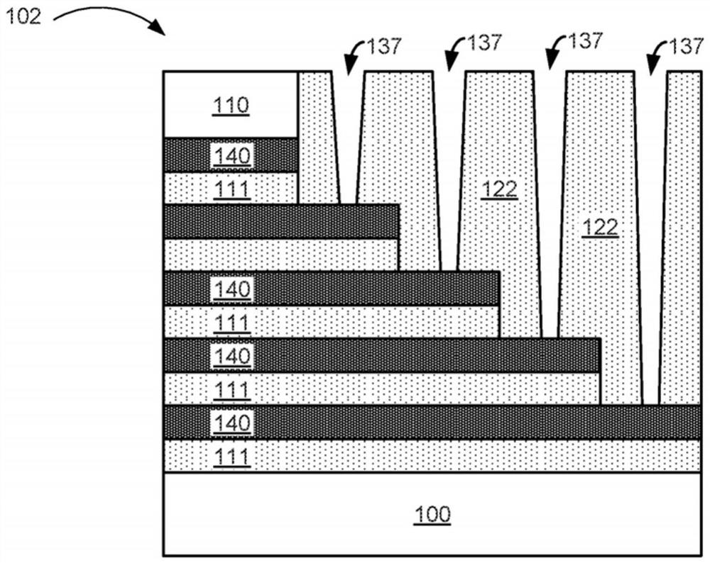
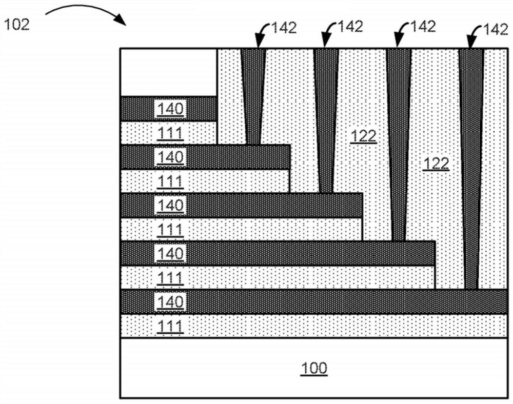
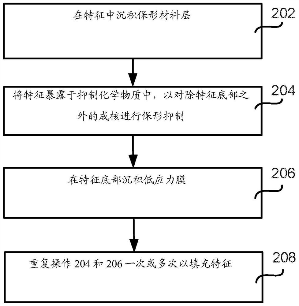
[0018] Described herein are methods of feature filling and related systems and apparatus. Examples of applications include logic and memory contact fill, DRAM buried word line fill, vertically integrated memory gate / word line fill, and 3-D integration using through-silicon vias (TSVs). In some implementations, the method can be used for tungsten feature fill. Such features may include vertical features, such as vias, and horizon...
PUM
 Abstract
Description
Claims
Application Information
 - R&D Engineer
- R&D Manager
- IP Professional
- Industry Leading Data Capabilities
- Powerful AI technology
- Patent DNA Extraction
Browse by: Latest US Patents, China's latest patents, Technical Efficacy Thesaurus, Application Domain, Technology Topic.
© 2024 PatSnap. All rights reserved.Legal|Privacy policy|Modern Slavery Act Transparency Statement|Sitemap