Method of integrating PEALD Ta-containing films into Cu metallization

a technology of ta-containing films and cu metallization, which is applied in the field of plasma enhanced atomic layer deposition for semiconductor manufacturing, can solve the problems of current ald process, affecting so as to improve the quality of deposited ald films, and reduce carbon conten

Inactive Publication Date: 2011-06-14
TOKYO ELECTRON LTD
View PDF14 Cites 56 Cited by
  • Summary
  • Abstract
  • Description
  • Claims
  • Application Information

AI Technical Summary

Benefits of technology

[0007]Accordingly, one object of the present invention is directed to improving the properties and integration of Ta-containing films in Cu metallization.

Problems solved by technology

In addition, plasma excitation may activate film-forming chemical reactions that are not energetically or kinetically favored in thermal CVD.
However, current ALD processes often suffer from contamination problems that affect the quality of the deposited ALD films, and the interfaces between the ALD films and other films in a manufactured device.
The presence of impurities in Ta-containing films can result in weak adhesion between a bulk Cu layer and the Ta-containing films, which in turn can result in electro-migration (EM) and stress migration (SM) problems, as well as reduced device production yields.

Method used


Image

  • Method of integrating PEALD Ta-containing films into Cu metallization
  • Method of integrating PEALD Ta-containing films into Cu metallization
  • Method of integrating PEALD Ta-containing films into Cu metallization

Examples


Embodiment Construction

[0022]In the following description, in order to facilitate a thorough understanding of the invention and for purposes of explanation and not limitation, specific details are set forth, such as a particular geometry of the deposition system and descriptions of various components. However, it should be understood that the invention may be practiced in other embodiments that depart from these specific details.

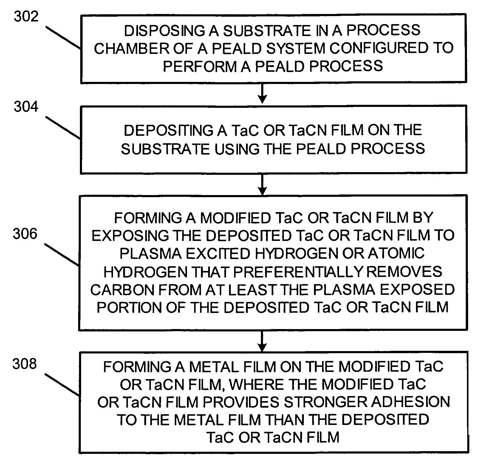
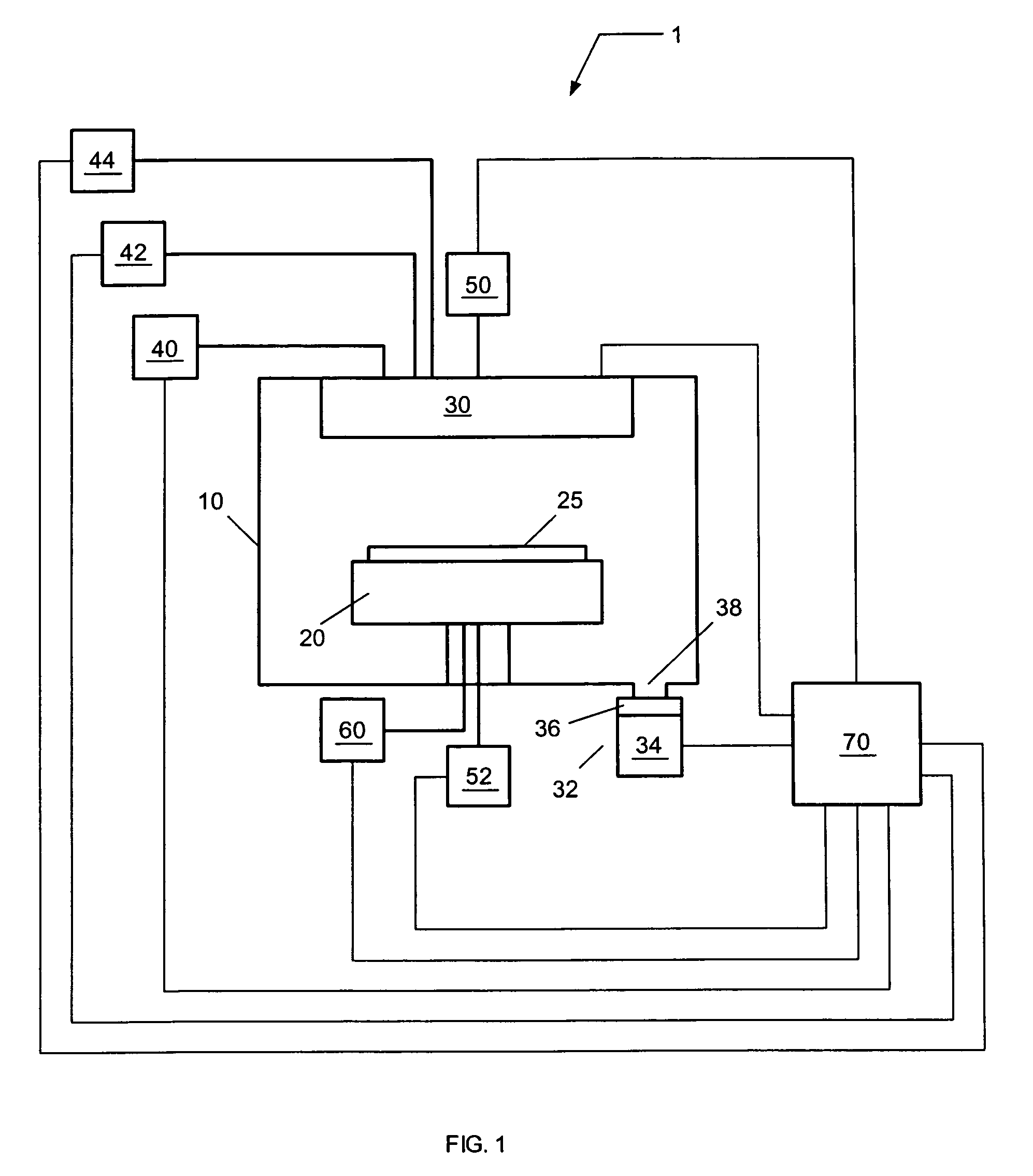
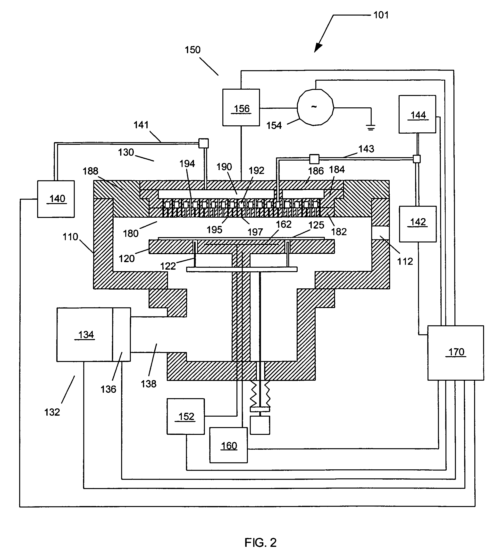
[0023]Referring now to the drawings, FIG. 1 illustrates a PEALD system 1 for depositing a thin TaC or TaCN film on a substrate according to one embodiment of the invention. For example, during the metallization of inter-connect and intra-connect structures for semiconductor devices in back-end-of-line (BEOL) operations, a thin conformal TaC or TaCN film may be deposited on wiring trenches or vias to minimize the migration of metal into the inter-level or intra-level dielectric, where the TaC or TaCN film provides acceptable adhesion to the dielectric and a Ru or Cu seed layers tha...


PUM

PropertyMeasurementUnit
thicknessaaaaaaaaaa
thicknessaaaaaaaaaa
thicknessaaaaaaaaaa

Abstract

A method for forming a modified TaC or TaCN film that may be utilized as a barrier film for Cu metallization. The method includes disposing a substrate in a process chamber of a plasma enhanced atomic layer deposition (PEALD) system configured to perform a PEALD process, depositing a TaC or TaCN film on the substrate using the PEALD process, and modifying the deposited TaC or TaCN film by exposing the deposited TaC or TaCN film to plasma excited hydrogen or atomic hydrogen or a combination thereof in order to remove carbon from at least the plasma exposed portion of the deposited TaCN film. The method further includes forming a metal film on the modified TaCN film, where the modified TaCN film provides stronger adhesion to the metal film than the deposited TaCN film. According to one embodiment, a TaCN film is deposited from alternating exposures of TAIMATA and plasma excited hydrogen.

Description

FIELD OF INVENTION[0001]The present invention relates to a method of plasma enhanced atomic layer deposition for semiconductor manufacturing, and more particularly to a method of forming Ta-containing films that may be utilized as a barrier layer in Cu metallization.BACKGROUND OF THE INVENTION[0002]Typically, during materials processing, plasma is employed to facilitate the addition and removal of material films when fabricating composite material structures. For example, in semiconductor processing, a (dry) plasma etch process is utilized to remove or etch material along fine trenches or within vias or contacts patterned on a silicon substrate. Alternatively, for example, a vapor deposition process is utilized to deposit material along fine lines or within vias or contacts on a silicon substrate. In the latter, vapor deposition processes include chemical vapor deposition (CVD), and plasma enhanced chemical vapor deposition (PECVD).[0003]In PECVD, plasma is utilized to alter or enha...

Claims


Application Information

Patent Timeline
Patent Type & Authority Patents(United States)
IPC IPC(8): C23C16/00H05H1/00
CPCC23C16/32C23C16/36C23C16/56C23C16/509C23C16/45542
Inventor ISHIZAKA, TADAHIROMATSUDA, TSUKASAHARA, MASAMICHIFAGUET, JACQUESMIZUSAWA, YASUSHI
Owner TOKYO ELECTRON LTD
Why Eureka
Try Eureka