Process for forming fine wiring

a technology of fine wires and wires, applied in the direction of liquid/solution decomposition chemical coating, metallic material coating process, coating, etc., can solve the problems of metal embossed, resultant device malfunction, etc., and achieve the effect of low resistance and good quality

Inactive Publication Date: 2001-09-25
RENESAS ELECTRONICS CORP
View PDF22 Cites 51 Cited by
  • Summary
  • Abstract
  • Description
  • Claims
  • Application Information

AI Technical Summary

Benefits of technology

Therefore, the present invention has been achieved in view of the above-mentioned problems. It is a main object of the present invention to provide a fine wiring and a process for manufacturing the same, which enables a uniform and good quality barrier metal film to be formed on a pattern side wall and its bottom in such a manner that the step overage is excellent without exposing the underlying layer or a pattern having a high aspect ratio of the wiring height to the wiring width or the distance between wirings.
It is another object of the present invention to provide a process which enables a fine wiring having a low resistance to be formed by uniformly loading a dominant wiring metal into a pattern on which a barrier metal is formed.
In the above-mentioned present invention, it is preferred that a plurality of metals which will form the barrier metal film or the wiring layer comprises a main metal and a metal to be added to the main metal. The metal to be added is selected from such a combination of metals such that the electrode potential required for reducing the metal to be added to ions is higher than a standard electrode potential required for reducing the film of the oxide or salt of the main metal to metal at the reducing step (b), whereby the metal to be added is removed as ions in the solution at the step (b) for reducing the plurality of metals which form metal oxide or metal salt film which becomes the barrier metal film or the wiring layer.

Problems solved by technology

When the dual damascene structure in which wirings and contacts are simultaneously formed is adopted to meet the requirements for high aspect ratio of trench wiring and multilayered wiring, embedding of a metal becomes more difficult.
This may cause malfunctions of the resultant device.

Method used


Image

  • Process for forming fine wiring
  • Process for forming fine wiring
  • Process for forming fine wiring

Examples


example 1

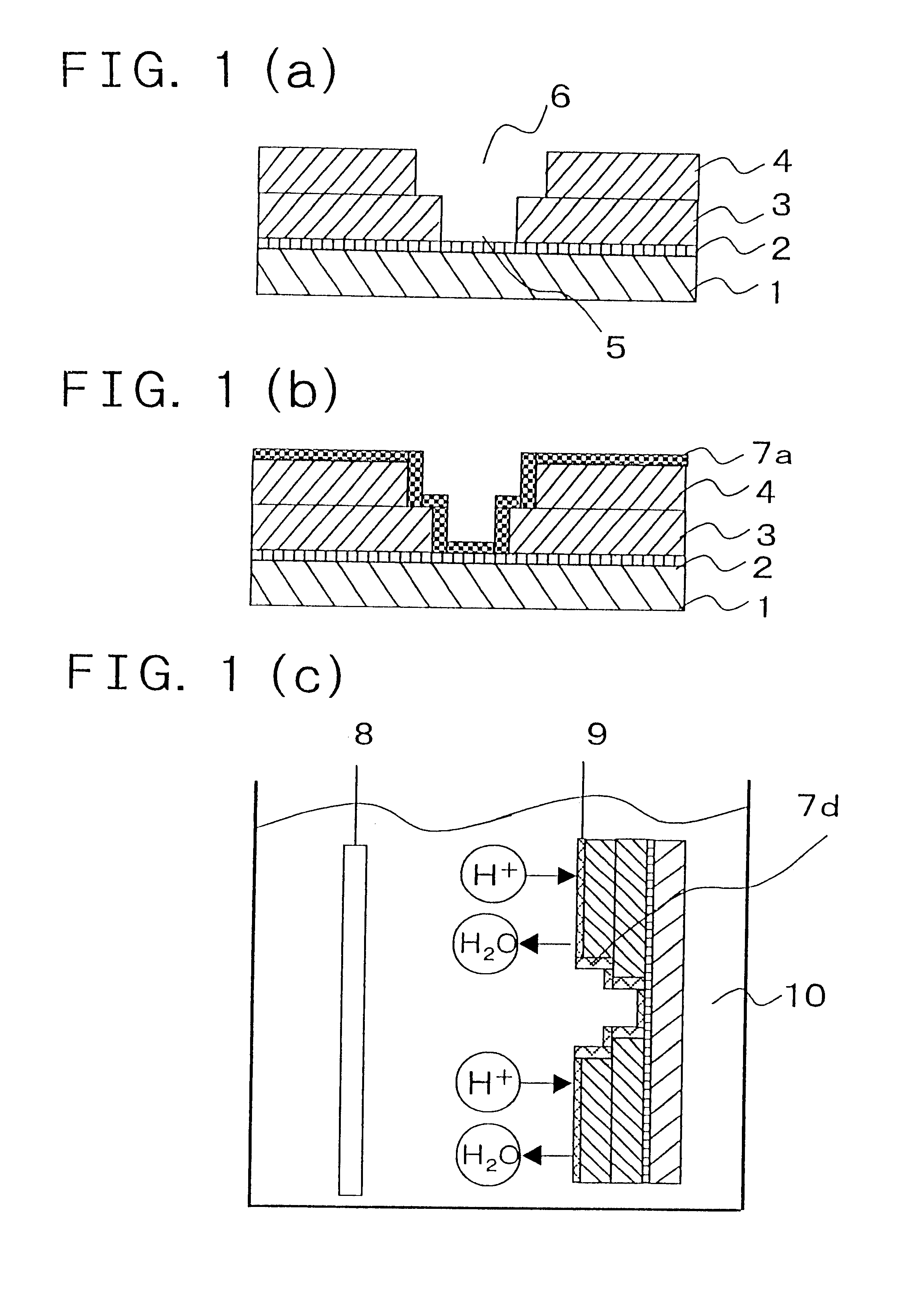
A first example of the present invention will now be explained. FIGS. 1 and 2 are schematic sectional views explaining the first example of the process for forming a fine wiring in accordance with the present invention. They are sectional views showing a sequence of steps of the process of forming the fine wiring. FIGS. 1 and 2 are divided for convenience of formulating of the drawing.

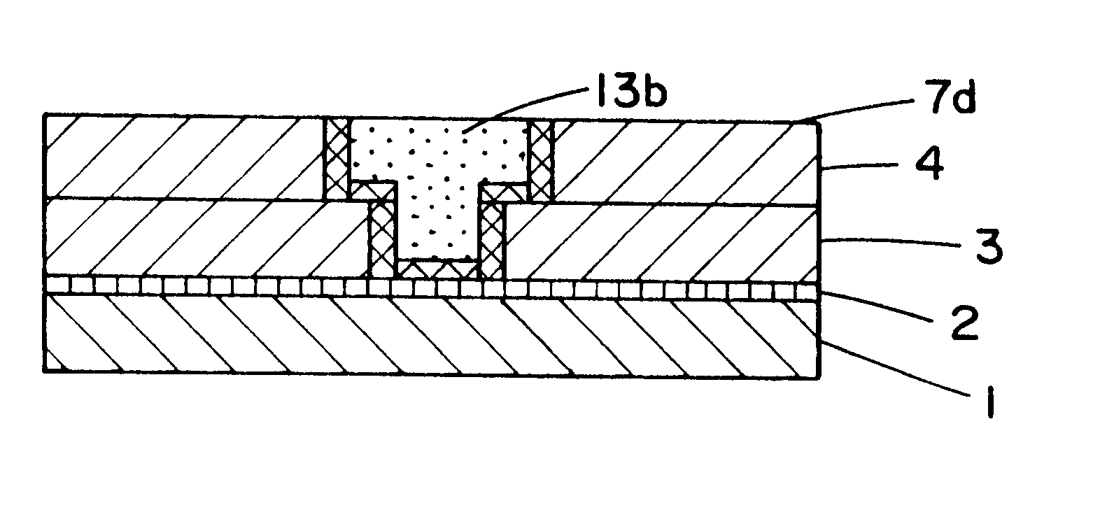
Referring now to FIG. 1, a lower layer wiring 2 is formed on a silicon substrate 1 in which elements such as transistors are formed. A first interlayer insulating film 3 having a thickness of 10 nm to 1000 nm is formed on the lower layer wiring 2 and a second interlayer insulating film 4 having a thickness of 10 nm to 1500 nm is formed on the film 3. At this time, these interlayer insulating films are formed by a CVD or coating process. Material to be used may include inorganic materials such as silicon oxide, fluorine-containing silicon oxide, polysilazane, hydrogensilsesquioxane, organic materials su...

example 2

A second example 2 of a process for forming fine wiring in accordance with the present invention will be described.

FIG. 3 is a schematic sectional view explaining the second example of the present invention. The second example 2 is identical with the first example 1 except that the plating step as shown in FIG. 2(d) in the latter example is replaced by an electroless plating step shown in FIG. 3 in the former example 1. The second example of the present invention will be described with reference to FIGS. 1 through 3.

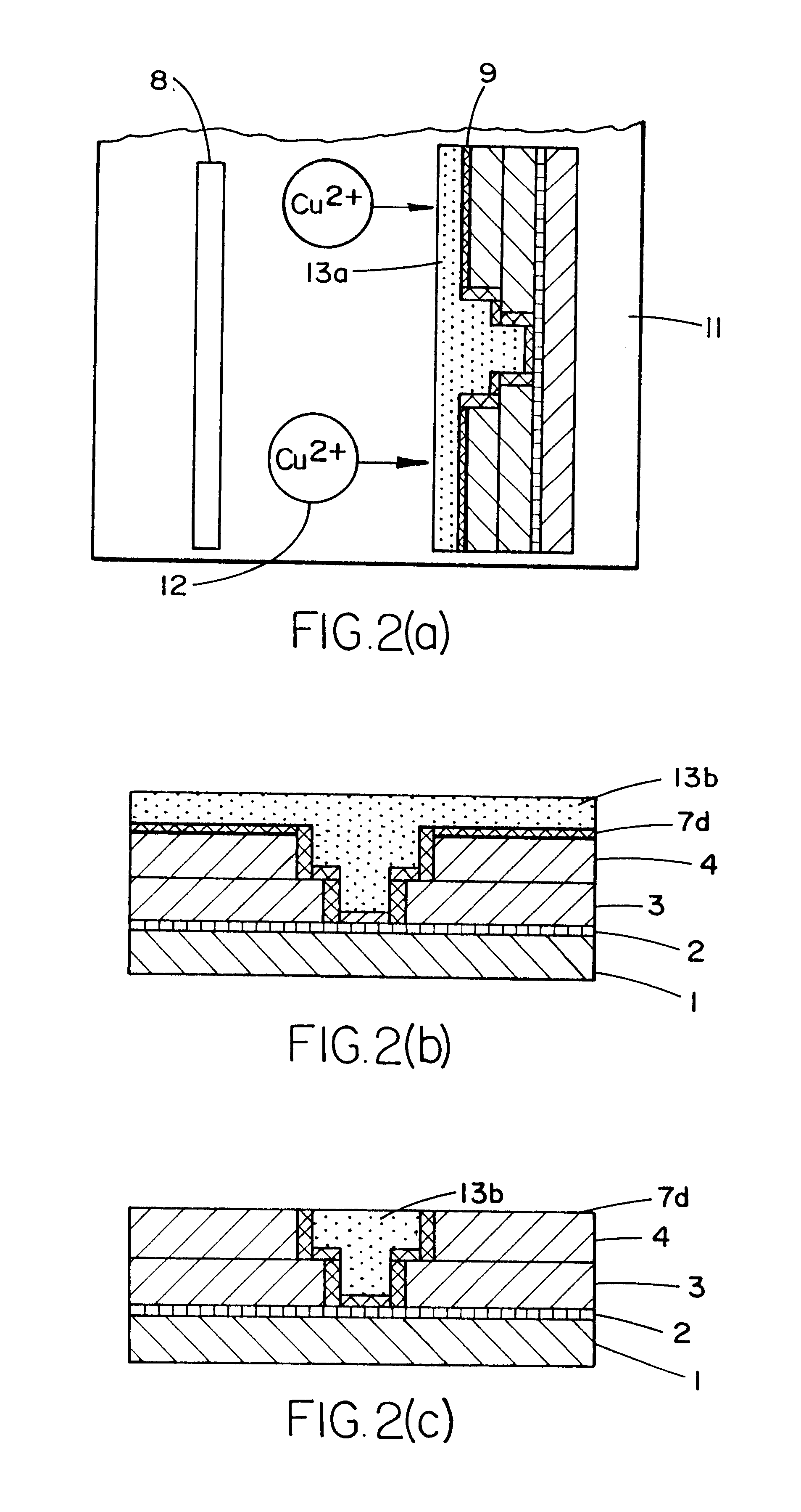
Referring now to FIG. 1, a pattern in which wiring material will be buried or embedded is formed as similarly to the first example. For example, a metal film 7a, e.g., tantalum oxide film is formed (FIG. 1(b)) and is then electrochemically reduced to a metal film e.g., tantalum 7d (FIG. 1(c)).

Referring now to FIG. 3, a substrate 1 having the metal film 7d, e.g., of tantalum film, thereon is dipped into an electroless plating bath 14 in which ions of copper such as copper...

first embodiment

A major difference between the first and second examples resides in that copper which will be a wiring material is formed by the electroless plating process after the film of a metal oxide which is excellent in coverage is reduced to the metal. An apparatus using the electroless plating process in the second example is lower in cost and enables more mass production in comparison with the A film having less pinholes can be formed over the entire of the substrate.

A third example of the present invention will be described. FIG. 4 is a schematic sectional view explaining the third example of the present invention. FIG. 4 shows, a step in the third example which is added between the reducing step as shown in FIG. 1(c) explaining the first example and the plating step of FIG. 2(d). The third example of the present invention will be described with reference to FIGS. 1, 2 and 4.

Referring now to FIG. 1, in the third Example of the present invention a pattern in which the wiring material is ...


PUM

PropertyMeasurementUnit
thicknessaaaaaaaaaa
thicknessaaaaaaaaaa
sizeaaaaaaaaaa

Abstract

The present invention is directed to a process for manufacturing a semiconductor device. It includes a step for forming a fine wiring, and provides a process for uniformly and positively forming a film of a barrier metal, such as tantalum, for preventing the metal, such as copper, which becomes the first material for the wiring, from diffusing into a silicon oxide film. The process involves depositing an oxide of a barrier metal on a substrate which is formed with a via hole by a process such as CVD process. A high quality barrier metal film is formed by reducing the oxide by applying a negative potential to the oxide in a solution in which hydrogen ions are present. Subsequently an embedded wiring is formed by embedding the main metal by a plating process and the like and polishing to remove unnecessary portions.

Description

The present invention relates to a process for forming a fine wiring for LSI, and in particular to a process for forming a fine wiring using a chemical vapor deposition process.Ever reducing design rule has become more strict to meet the requirements to increase the scale of integration and speed of the LSI. Reduction in wiring pitch has led to reduction in the width of wiring and distance between the wirings. However, reduction in thickness of wiring has not been largely achieved in comparison with the reduction in wiring pitch in order to prevent an increase in resistance of wiring.Accordingly, the aspect ratio of the wiring height to the wiring width or distance between wirings tends to increase. Embedding of metal has become more difficult in particular when trench wiring is used. Similarly, the aspect ratio of via for connecting with an active area or underlying wiring has also increased, so that embedding of metal has become more difficult.Efforts to use materials having a low...

Claims


Application Information

Patent Timeline
Patent Type & Authority Patents(United States)
IPC IPC(8): H01L21/768H01L21/70H01L21/3205C23C18/31H01L21/288
CPCH01L21/76823H01L21/76826H01L21/76843H01L21/76877H01L21/76859H01L21/76861H01L21/76873H01L21/76856H01L21/28
Inventor YOKOYAMA, TAKASHIKISHIMOTO, KOJI
Owner RENESAS ELECTRONICS CORP
Why Eureka
Try Eureka