Process for Fabricating Nanowire Arrays

a nanowire array and nanotechnology technology, applied in the field of nanotechnology, can solve the problems of limited scalability of nanowire synthesis, high temperature and/or low pressure, and many nanosystems that are not utilized commercially

Active Publication Date: 2009-10-15
ADVANCED SILICON GRP TECH LLC
View PDF7 Cites 55 Cited by
  • Summary
  • Abstract
  • Description
  • Claims
  • Application Information

AI Technical Summary

Problems solved by technology

Today, many nanosystems are not utilized commercially due to the large cost associated with fabrication, and limitations in the scalability of nanowire synthesis.
These systems require high temperature and / or low pressure which is largely responsible for the high cost.
The ultimate diameter achieved with this technique has been limited.

Method used


Image

  • Process for Fabricating Nanowire Arrays
  • Process for Fabricating Nanowire Arrays
  • Process for Fabricating Nanowire Arrays

Examples


Embodiment Construction

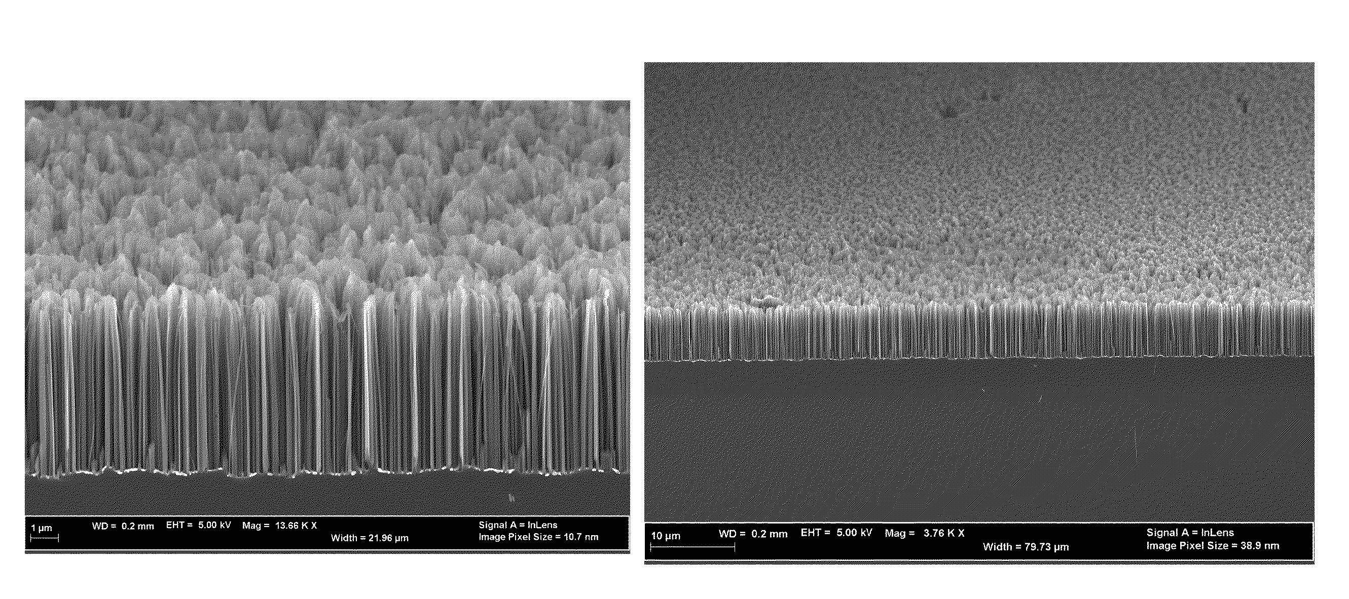
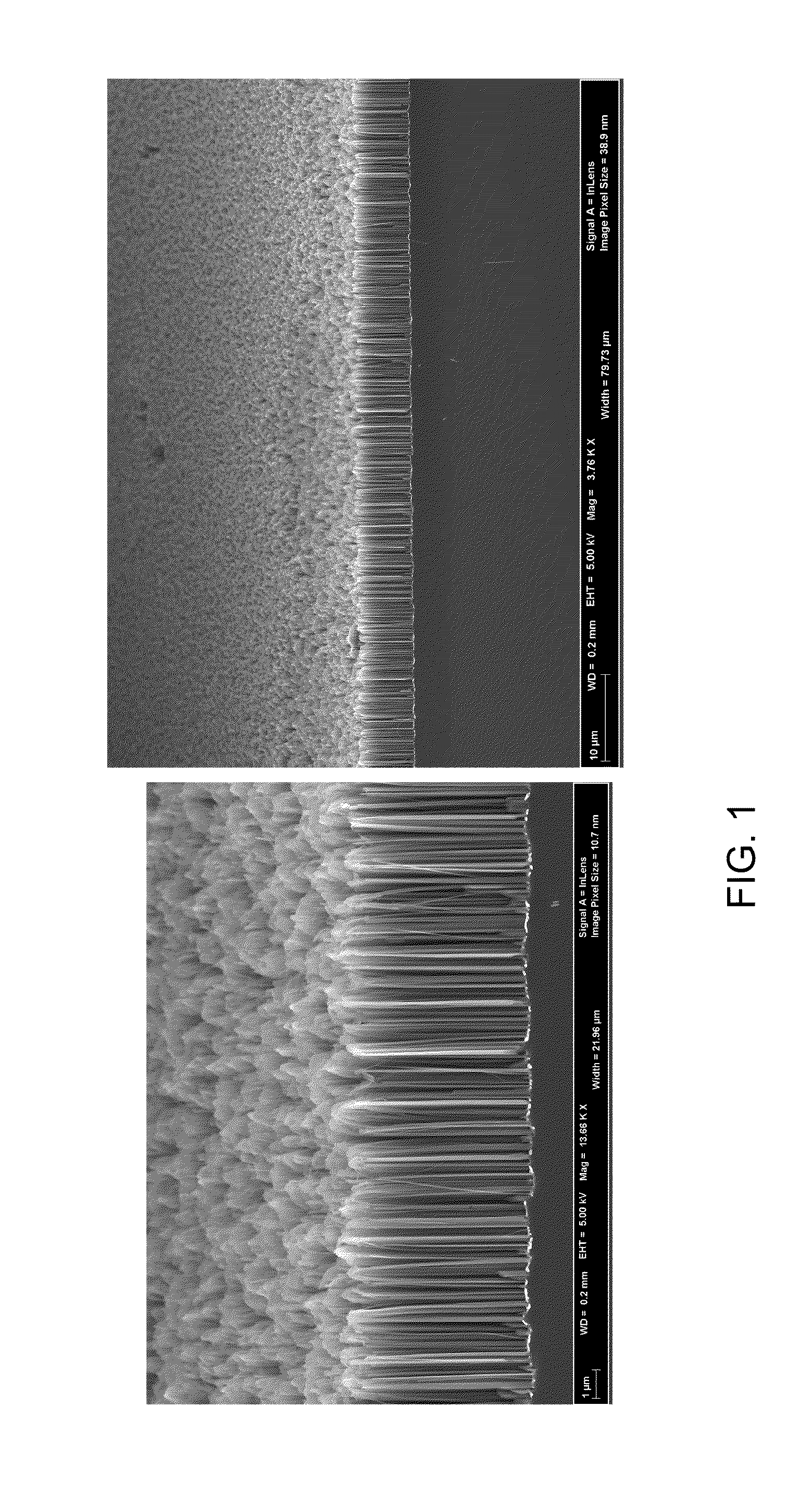
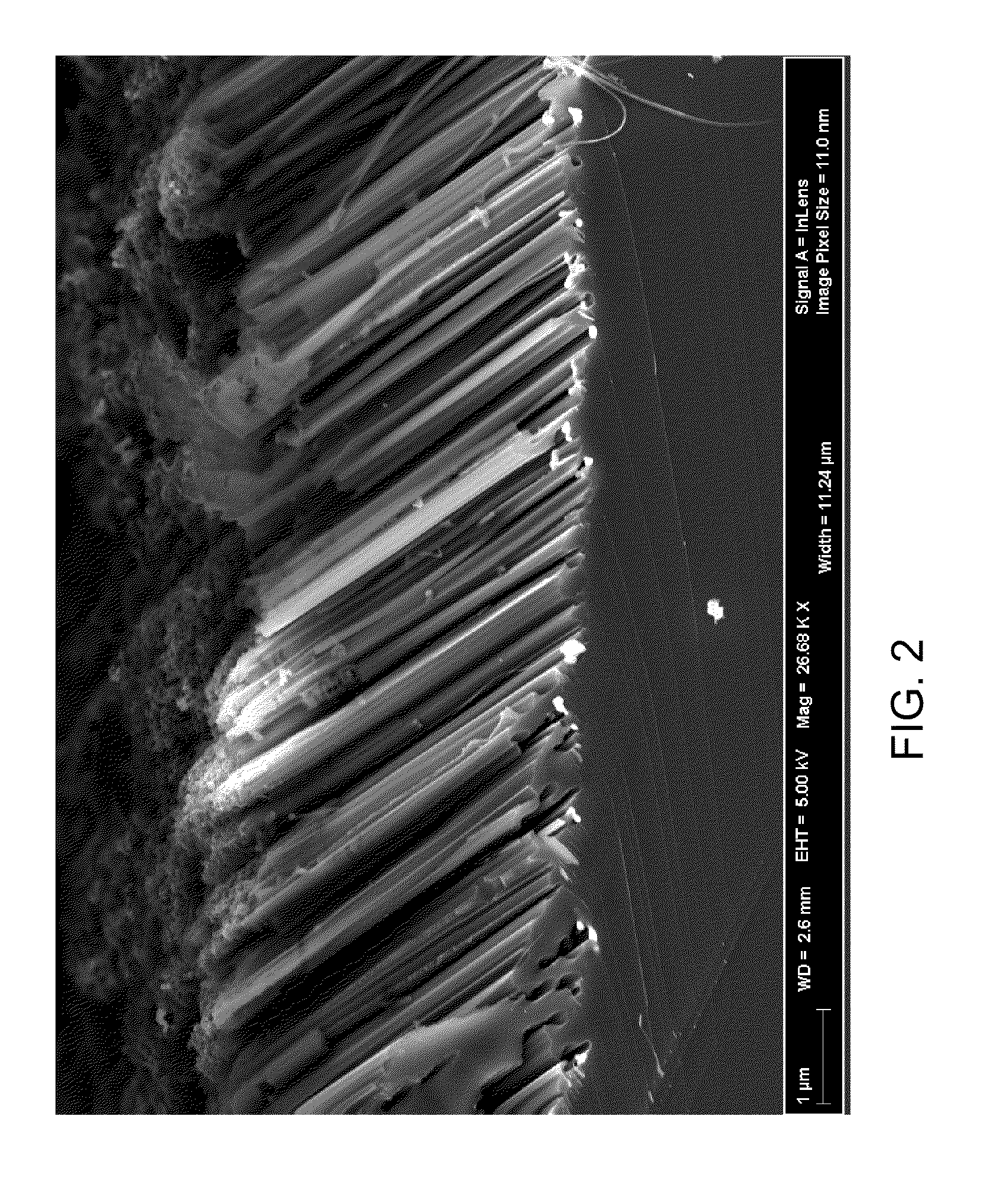
[0013]In an aspect of the invention, a process is provided for etching a silicon-containing substrate to form nanostructures. In this process, one deposits and patterns a metal film onto the substrate in such a way that the metal is present and touches silicon where etching is desired and is blocked from touching silicon or not present elsewhere. One submerges the metallized substrate into an etchant aqueous solution comprising about 4 to about 49 weight percent HF and an oxidizing agent.

[0014]In a process as described above, to achieve sub-100 nm nanowires, one may use sub-100 nm nanoparticles to block the silver from the silicon. The nanoparticles may be made of a variety of substances, for example silicon dioxide, iron oxide, or polymers.

[0015]A. First Exemplary Process

[0016]An exemplary process utilizes the spinning of SiO2 nanoparticles well dispersed in an isopropanol solution (5 wt % SiO2 in IPA) that ranged in particle size from 12-30 nm at 4000 RPM. Subsequent to spin-coati...


PUM

PropertyMeasurementUnit
diametersaaaaaaaaaa
diameteraaaaaaaaaa
diameteraaaaaaaaaa

Abstract

A process is provided for etching a silicon-containing substrate to form nanowire arrays. In this process, one deposits nanoparticles and a metal film onto the substrate in such a way that the metal is present and touches silicon where etching is desired and is blocked from touching silicon or not present elsewhere. One submerges the metallized substrate into an etchant aqueous solution comprising HF and an oxidizing agent. In this way arrays of nanowires with controlled diameter and length are produced.

Description

CROSS-REFERENCE TO RELATED APPLICATIONS[0001]The present application claims priority to U.S. Provisional Applications Nos. 61 / 044,573, filed Apr. 14, 2008, and 61 / 141,082, filed Dec. 29, 2008. These applications are incorporated by reference herein.TECHNICAL FIELD[0002]This application pertains to the field of nanotechnology.BACKGROUND OF THE INVENTION[0003]The ability to structure and pattern silicon is important for many applications. There has been particular interest in patterning silicon to make nanostructures. Relevant information regarding silicon fabrication processes known to those of skill in the art can be found, for example, in Sami Franssila, Introduction to Microfabrication (John Wiley & Sons, 2004), and the references cited there.[0004]Semiconductor nanowires have become the focal point of research over the last decade due to their interesting physical, chemical and biological properties. There is particular interest surrounding silicon nanowires, as silicon is one of...

Claims


Application Information

Patent Timeline
Patent Type & Authority Applications(United States)
IPC IPC(8): H01L29/15H01L29/06H01L29/04H01L21/306H01L21/20H01L33/00H01L31/036B01J20/02
CPCB01J20/10H01M10/0525B82Y20/00B82Y30/00H01L21/30604H01L21/3086H01L31/0236H01M4/134H01M4/1395H01M4/366H01M4/386H01M4/661Y02E10/50Y10S977/762H01L29/0676H01L29/16B01J20/28007H01L31/02363C23C14/34H01L21/02118H01L21/02164H01L21/02175H01L21/02244H01L21/02282H01L21/02307H01L21/0234H01L21/02488H01L21/02513H01L21/02532H01L21/02603H01L21/2855H01L21/28568H01L21/32134H01L29/04H01L29/0669H01L31/028H01L31/0352H01M4/0492H01M2004/027
Inventor BUCHINE, BRENT A.MODAWAR, FARISBLACK, MARCIE R.
Owner ADVANCED SILICON GRP TECH LLC
Why Eureka
Try Eureka