Chip mounting process capable for reducing stress

It is a technology of chip mounting and surface mounting technology, which is applied in the manufacture of electrical components, electrical solid devices, semiconductor/solid devices, etc. It can solve problems such as broken interconnection solder balls, increased difficulty of chip consistency, and inability to realize folding or bending. , to achieve the effect of reducing stress and solving terminal reliability problems

Active Publication Date: 2021-07-27
浙江集迈科微电子有限公司
View PDF10 Cites 0 Cited by
  • Summary
  • Abstract
  • Description
  • Claims
  • Application Information

AI Technical Summary

Problems solved by technology

[0002] Integrated circuit terminals are increasingly developing towards large-size chips. These two areas will have the following problems in terminal packaging and interconnection technologies: First, large-size chips will be subject to stress from the base during surface mounting. In the high and low temperature failure test, the large-size chip has a different thermal expansion coefficient from the base, which often leads to the breakage of the interconnection solder balls. If it is a three-dimensional package, then the adapter plate between the chip and the base will break. ;Flexible circuits need to match various usage environments. For wearable flexible circuits, if the size of the chip mounted on it is too large, it cannot be folded or bent at certain angles, which seriously affects the range of use of the terminal.
[0003] At present, in order to achieve high integration of some applications in the industry, it is necessary to mount arrayed small chips to replace the large chips that were originally to be mounted. This not only increases the difficulty of consistency between chips, but also increases the number of mounting times and mounting costs. , also increases the overall chip area

Method used


Image

  • Chip mounting process capable for reducing stress
  • Chip mounting process capable for reducing stress
  • Chip mounting process capable for reducing stress

Examples


Embodiment 1

[0040] Embodiment 1, in this embodiment, a stress-reducing chip mounting process includes the following steps:

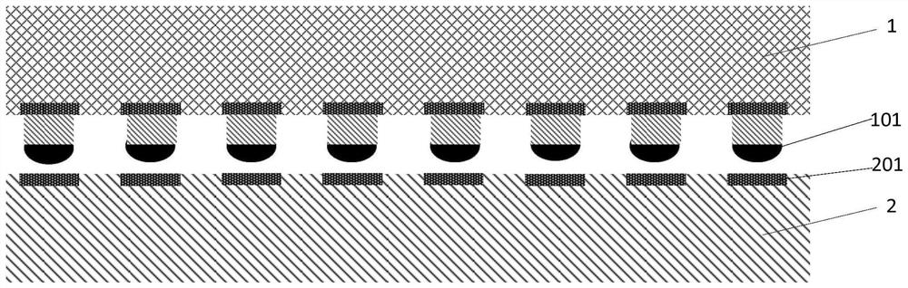
[0041] Step S1, the chip 1 is mounted on the surface of the substrate 2 through the surface mount process, and the solder balls 101 on the front of the chip 1 are connected to the pads 201 on the substrate 2 by reflow soldering; the chip 1 is preset with an array of small chip unit;

[0042] Specifically, such as Figure 1a As shown, pads 201 and wiring are distributed on the surface of the substrate 2, solder balls 101 for interconnection have been prepared on the front of the chip 1, and the chip 1 and the substrate 2 are welded by reflow soldering; the material of the substrate 2 is a PCB board, or a ceramic substrate , plastic substrates, etc.;

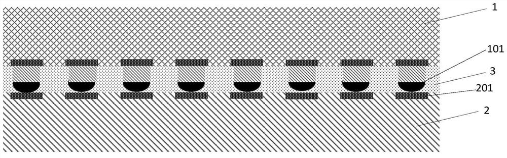
[0043] Step S2, filling the underfill glue 3 at the bottom of the chip 1, absorbing the liquid underfill glue 3 into the gap between the chip 1 and the substrate 2 through the surface tension of the chip 1 and the subs...

Embodiment 2

[0048] Embodiment 2, in this embodiment, a stress-reducing chip mounting process includes the following steps:

[0049] Step S1, the chip 1 is mounted on the surface of the substrate 2 through the surface mount process, and the solder balls 101 on the front of the chip 1 are connected to the pads 201 on the substrate 2 by reflow soldering; the chip 1 is preset with an array of small chip unit;

[0050] Specifically, such as Figure 1a As shown, it is the same as step S1 in Embodiment 1;

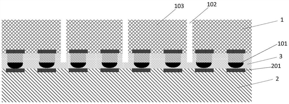
[0051] Step S2, splitting from the back of the chip 1 to form grooves 102, and splitting the chip 1 into array-type small chip units 103; interconnection;

[0052] Specifically, the chip 1 can be divided into an array of small chip units 103 by photolithography and dry etching; or, the chip 1 can be divided into an array of small chip units 103 by blade cutting or laser cutting; the formed The trench 102 can be as Figure 2a or Figure 2b shown;

[0053] Step S3, filling the underfill glu...

Embodiment 3

[0055] Embodiment 3, in this embodiment, a stress-reducing chip mounting process includes the following steps:

[0056] Step S1, making a groove 102 on the front of the chip 1, the groove 102 does not penetrate the material of the chip 1; the chip 1 is preset with an array of small chip units;

[0057] Specifically, the groove 102 can be made by dry etching, blade cutting or laser cutting;

[0058] In step S2, the chip 1 is mounted on the surface of the substrate 2 through a surface mount process, and the solder balls 101 on the front of the chip 1 are connected to the pads 201 on the substrate 2 by reflow soldering;

[0059] The material of the substrate 2 is a PCB board, and can also be a ceramic substrate, a plastic substrate, etc.;

[0060] Step S3, grinding or dry etching the back of the chip 1, so that the prefabricated groove 102 penetrates through the material of the remaining thickness of the chip 1, thereby dividing the chip 1 into an array of small chip units 103; ...


PUM


Abstract

The invention provides a chip mounting process for reducing stress. The process comprises the following steps of S1, mounting a chip on the surface of a substrate through a surface mounting process, and performing reflow soldering to correspondingly connect each solder ball on the front surface of the chip with a bonding pad on the substrate, wherein the chip is provided with array type small chip units in advance; S2, filling the bottom of the chip with underfill glue, absorbing the liquid underfill glue to enter a gap between the chip and the substrate through the surface tension of the chip and the substrate, and then curing the underfill glue; S3, segmenting the back surface of the chip to form a groove, and segmenting the chip into the array type small chip units, wherein the small chip units realize the interconnection among the array type small chip units through the bonding pads and wires on the substrate. According to the invention, the chip is designed into an array structure, the chip is welded with the substrate and is divided into the array small chip units, so that the chip mounting consistency difficulty can be reduced, the mounting cost is reduced, and the total area of the chip is kept basically unchanged.

Description

technical field [0001] The invention relates to the technical field of semiconductors, in particular to a stress-reducing chip mounting process. Background technique [0002] Integrated circuit terminals are increasingly developing towards large-size chips. These two areas will have the following problems in terminal packaging and interconnection technologies: First, large-size chips will be subject to stress from the base during surface mounting. In the high and low temperature failure test, the large-size chip has a different thermal expansion coefficient from the base, which often leads to the breakage of the interconnection solder balls. If it is a three-dimensional package, then the adapter board between the chip and the base will break. ; Because flexible circuits need to match various usage environments, for wearable flexible circuits, if the size of the chip mounted on it is too large, it cannot be folded or bent at certain angles, which seriously affects the range o...

Claims


Application Information

Patent Timeline
Patent Type & Authority Applications(China)
IPC IPC(8): H01L21/50H01L21/56
CPCH01L21/50H01L21/56H01L24/81H01L2224/81815
Inventor 冯光建郭西顾毛毛黄雷高群
Owner 浙江集迈科微电子有限公司
Why Eureka
Try Eureka