Semiconductor structure

A semiconductor and restricted area technology, which is applied in the direction of semiconductor devices, microstructure technology, semiconductor/solid-state device components, etc., can solve problems that affect the structural performance of MEMS speaker packages, complex manufacturing processes, and difficult sealing.

Pending Publication Date: 2021-08-03
ADVANCED SEMICON ENG INC
View PDF0 Cites 0 Cited by
  • Summary
  • Abstract
  • Description
  • Claims
  • Application Information

AI Technical Summary

Problems solved by technology

However, since the seal ring and the solder material connecting the MEMS and the substrate are made by different processes, the manufacturing process is more complicated. In addition, if there is a warpage problem between the substrate and the MEMS, the sealing ring is not easy for the substrate and the substrate. A seal is formed between MEMS, and even the sound hole is covered because the flow is not easy to control, which affects the performance of the MEMS speaker package structure

Method used


Image

  • Semiconductor structure
  • Semiconductor structure
  • Semiconductor structure

Examples


Embodiment Construction

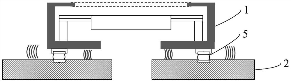
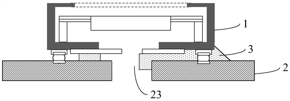
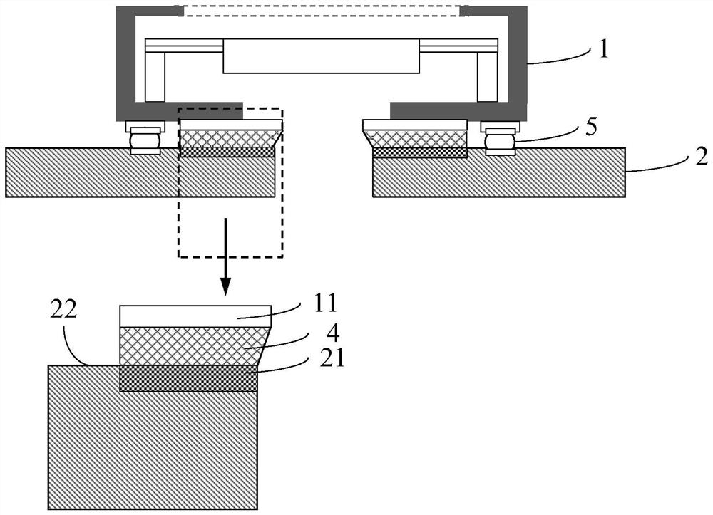
[0030] The specific implementations of the present disclosure will be described below with reference to the accompanying drawings and embodiments, and those skilled in the art can easily understand the technical problems solved by the present disclosure and the technical effects produced by the content described in this specification. It should be understood that the specific embodiments described herein are only used to explain the related invention, but not to limit the invention. In addition, for the convenience of description, only the parts related to the related invention are shown in the drawings.

[0031] It should be noted that the structures, proportions, sizes, etc. shown in the drawings in the description are only used to cooperate with the contents described in the description for the understanding and reading of those skilled in the art, and are not intended to limit the implementation of the present disclosure. Restricted conditions, so it does not have technica...


PUM


Abstract

The invention relates to a semiconductor structure. A limiting region of a sealing material is formed by a hydrophobic material and a hydrophilic material, the problem that the sealing material is not prone to control is solved, the performance of the product is improved, and the yield of the product is increased.

Description

technical field [0001] The present disclosure relates to the field of semiconductor technology, and in particular, to semiconductor structures. Background technique [0002] With the evolution of packaging technology, various packaging structures have been introduced, and the overall package size has become smaller and smaller. Micro-electromechanical systems (MEMS, Micro-Electro-Mechanical System) are the integration of semiconductors and precision machinery. Sensors and microactuators communicate with the external environment, which in turn links other mechanism behaviors. Now, the MEMS packaging structure has the advantages of high strength, high performance and low price, which is the focus of the future. [0003] The traditional MEMS speaker package structure is usually designed with a seal ring at the substrate end or the MEMS end to prevent sound waves from interfering with in-phase sound waves after reflection (ie, anti-phase sound waves interfering with in-phase so...

Claims


Application Information

Patent Timeline
Patent Type & Authority Applications(China)
IPC IPC(8): B81B7/00B81B7/02B81C1/00
CPCB81B7/0032B81B7/02B81C1/00261
Inventor 叶昶麟
Owner ADVANCED SEMICON ENG INC
Why Eureka
Try Eureka