Device and method for detecting warping degree of wafer

A warpage and position detection technology, which is applied in the field of warpage devices, can solve problems such as scratches or collisions, increased deviation of test result data, and inability to detect wafer warpage

Active Publication Date: 2021-08-03
BEIJING NAURA MICROELECTRONICS EQUIP CO LTD
View PDF13 Cites 0 Cited by
  • Summary
  • Abstract
  • Description
  • Claims
  • Application Information

AI Technical Summary

Problems solved by technology

However, the AWC sensor cannot detect the change in the height of the wafer in the vertical direction, that is, it cannot detect whether the wafer is warped. If the warped wafer enters the next transmission link, it is prone to scratches or collisions.
Moreover, when the warped wafer is detected by the AWC sensor, it is easy to cause the deviation of the detection result data to increase. In severe cases, the AWC detection alarm will be triggered, indicating that the deviation of the wafer displacement is too large. The deviation of the actual horizontal position caused by the position, or the vertical height deviation caused by the shape warping of the wafer, can only be alarmed and shut down for equipment maintenance and taking slices

Method used


Image

  • Device and method for detecting warping degree of wafer
  • Device and method for detecting warping degree of wafer
  • Device and method for detecting warping degree of wafer

Examples


Embodiment 1

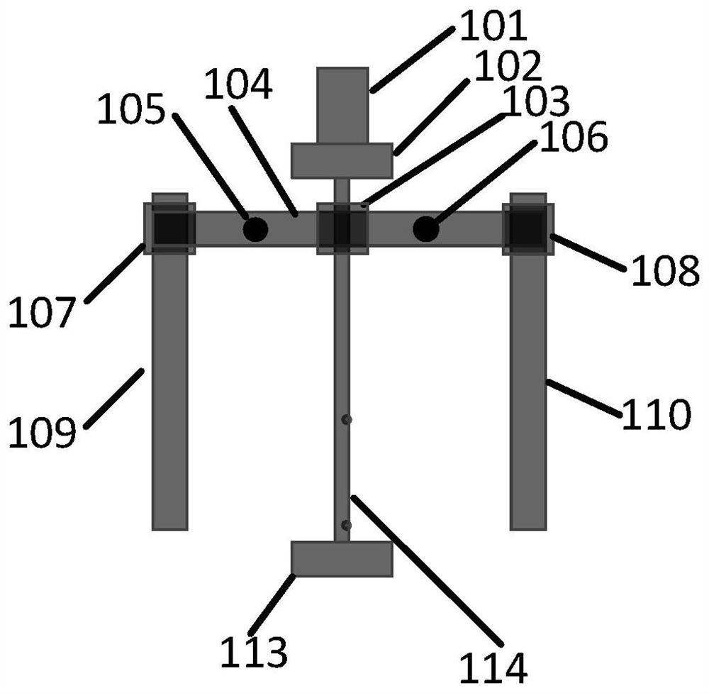
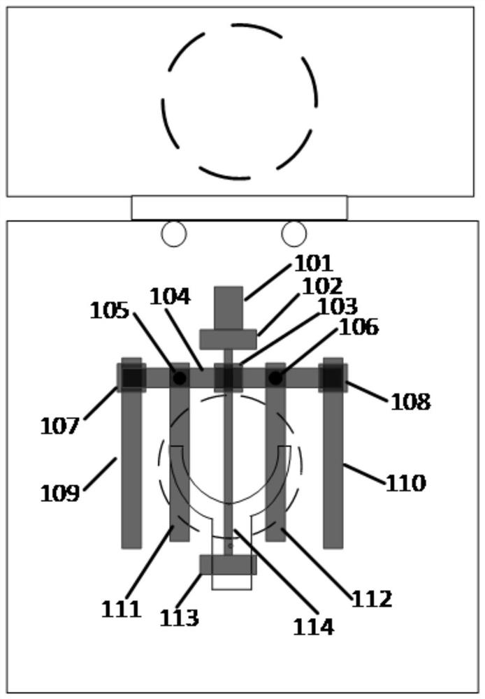
[0109] Such as Figure 1 to Figure 4 As shown, the present invention provides a device for detecting the warpage of a wafer. The wafer is placed on a carrier device in a transport chamber. The detection device includes a beam 104, a pair of distance measuring sensors 105, a driving device and Processor; where,

[0110] The beam 104 is arranged on the upper cover of the transmission chamber, and a pair of ranging sensors 105 are arranged on the beam 104;

[0111] The driving device is used to drive the crossbeam 104 to move in the horizontal direction relative to the plane where the wafer is located, and drive the ranging sensor 105 to move to detect the distance between the detection end of the ranging sensor 105 and the wafer;

[0112] The processor is used to calculate the warpage of the wafer according to the distance detected by the pair of distance measuring sensors 105, and give an alarm when the warpage exceeds a preset deviation.


PUM


Abstract

The invention discloses a device and method for detecting the warping degree of a wafer. The wafer is placed on a bearing device in a transmission chamber, and the detection device comprises a cross beam, a pair of distance measuring sensors, a driving device and a processor, wherein the cross beam is arranged on an upper cover of the transmission chamber, and the distance measuring sensors are arranged on the cross beam; the driving device is used for driving the cross beam to move in the horizontal direction relative to the plane where the wafer is located and driving the distance measuring sensor to move so as to detect the distance between the detection end of the distance measuring sensor and the wafer; and the processor is used for calculating the warping degree of the wafer according to the distance detected by the distance measuring sensors. According to the device for detecting the warping degree of the wafer, the driving device drives the cross beam to drive the distance measuring sensor to move so as to detect the distance between the detection end of the distance measuring sensor and the wafer, and the processor calculates the warping degree of the wafer according to the detection result so as to judge whether the wafer is warped or not, and the direct alarm and shutdown when the AWC test exceeds the deviation are avoided.

Description

technical field [0001] The invention belongs to the technical field of semiconductors, and more specifically relates to a device and a detection method for detecting the warpage of a wafer. Background technique [0002] Chemical vapor deposition epitaxial growth is to transport the reaction gas to the reaction chamber, and react it by heating, etc., and the growth atoms are deposited on the substrate to grow a single crystal layer. When the wafer is picked up after the epitaxial process is completed, the temperature of the wafer is about 800°C. In this state, since the diameter of the 12-inch wafer is 300mm, obvious deformation and warpage will occur after the process. In the prior art, the manipulator picks up the wafer from the process chamber and transfers it to the transfer chamber. The end face of the process chamber towards which the manipulator moves is equipped with a wafer automatic centering (Active Wafer Cekterikg, AWC) detection mechanism, that is, on the left s...

Claims


Application Information

Patent Timeline
Patent Type & Authority Applications(China)
IPC IPC(8): H01L21/66G01B11/02G01B11/24C23C16/52
CPCH01L22/12G01B11/02G01B11/24C23C16/52
Inventor 商家强
Owner BEIJING NAURA MICROELECTRONICS EQUIP CO LTD
Why Eureka
Try Eureka