
Wafer clamping device for single-wafer wet cleaning process cavity

A technology of wet cleaning and process chamber, which is applied in the direction of chemical instruments and methods, cleaning methods and utensils, cleaning methods using liquids, etc., to achieve the effect of reducing particle defects and reducing adverse effects

Active Publication Date: 2021-08-06
HUA HONG SEMICON WUXI LTD
View PDF6 Cites 0 Cited by
  • Summary
  • Abstract
  • Description
  • Claims
  • Application Information

AI Technical Summary

Problems solved by technology

[0003] The technical problem to be solved by the present invention is to provide a wafer clamping device for a single-chip wet cleaning process chamber, which can fix the wafer very well by using the thimble clamping method, and at the same time can reduce the impact of the thimble pin on the flow of cleaning liquid on the wafer surface. detrimental effect, thereby reducing particle defects on the wafer surface

Method used


Image

  • Wafer clamping device for single-wafer wet cleaning process cavity
  • Wafer clamping device for single-wafer wet cleaning process cavity
  • Wafer clamping device for single-wafer wet cleaning process cavity

Examples


no. 1 example

[0055] The wafer clamping device of the single-chip wet cleaning process chamber according to the first embodiment of the present invention:

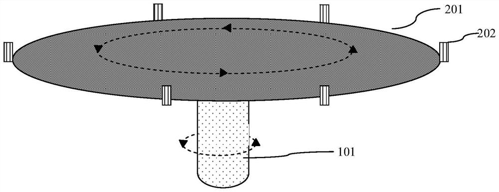
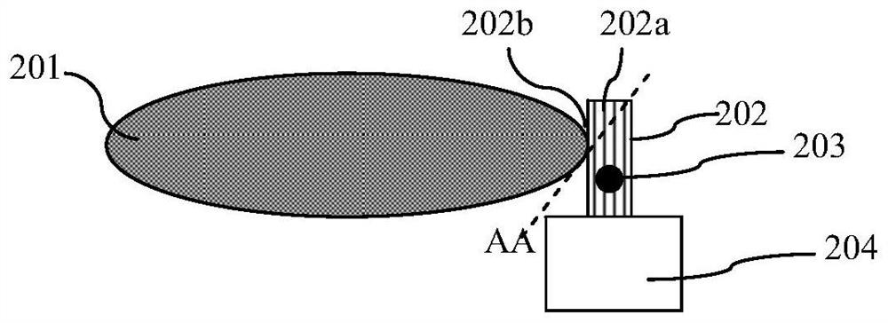
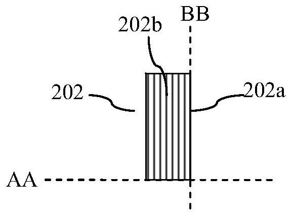
[0056] Such as Figure 5A As shown, it is an enlarged schematic diagram of the structure of a thimble 302 when the wafer clamping device of the single-wafer wet cleaning process chamber in the first embodiment of the present invention is in a clamped state; Figure 5B yes Figure 5A A schematic structural view of the thimble 302 viewed toward the contact surface 302b of the thimble 302; Figure 6 As shown, it is an enlarged schematic diagram of the structure of a thimble 302 when the wafer clamping device of the single-chip wet cleaning process chamber in the first embodiment of the present invention is in the open state; the overall structure of the single-chip wet cleaning process chamber provided by the present invention Please also refer to figure 1 As shown; the wafer clamping device of the single-chip wet cleaning process chamb...

no. 2 example

[0078] The wafer clamping device of the single-chip wet cleaning process chamber according to the second embodiment of the present invention:

[0079] The difference between the wafer clamping device of the single-chip wet cleaning process chamber of the second embodiment of the present invention and the wafer clamping device of the single-chip wet cleaning process chamber of the first embodiment of the present invention is that the second embodiment of the present invention The wafer clamping device of the monolithic wet cleaning process chamber also has the following features:

[0080] Such as Figure 7A As shown, it is a perspective view of the size gradient structure of the thimble 302 of the wafer clamping device of the single-chip wet cleaning process chamber according to the second embodiment of the present invention; Figure 7B As shown, it is a front view along the contact surface 302b of the size gradient structure of the thimble 302 of the wafer clamping device of ...


PUM


Abstract

The invention discloses a wafer clamping device of a single-wafer wet cleaning process cavity. The wafer clamping device comprises a plurality of ejector pins; each ejector pin is provided with a contact surface making contact with the edge of a wafer and side surfaces located on two sides of the contact surface, and the side surface on the upstream side in the rotation direction is a first side surface. When the wafer is clamped and fixed to a turntable device, the edge of the wafer makes contact with the contact surface, and the first side surface and the tangent line of the edge of the wafer form an acute angle so as to form a structure which is beneficial for cleaning liquid to flow in the contact position of the ejector pins and the edge of the wafer. The wafer can be well fixed in an ejector pin clamping mode, meanwhile, the adverse effect of the ejector pins on flowing of the cleaning liquid on the surface of the wafer can be reduced, and thus the particle defect on the surface of the wafer can be reduced.

Description

technical field [0001] The invention relates to a semiconductor integrated circuit manufacturing equipment, in particular to a wafer chucking device for a single-chip wet cleaning (single clean) process chamber. Background technique [0002] In the single-wafer wet cleaning process chamber, it is often necessary to use a wafer clamping device to fix the wafer. The wafer clamping methods include vacuum adsorption, electrostatic adsorption, and pin clamping. In a single-wafer wet cleaning process chamber similar to a single-wafer wet cleaning machine, the wafer is often fixed by clamping the wafer from the edge of the wafer with a thimble. For example, in the production of Al wiring in the back-end process (BEOL), it is necessary to use a cleaning solution with a model number of NE111 for cleaning. At this time, it is necessary to use a single-chip wet cleaning equipment for cleaning. In the mainstream single-wafer wet cleaning equipment, the key technology is the design of t...

Claims


Application Information

Patent Timeline
Patent Type & Authority Applications(China)
IPC IPC(8): B08B3/02B08B13/00H01L21/67
CPCB08B3/022B08B13/00H01L21/6708H01L21/67051
Inventor 李春元王泽飞
Owner HUA HONG SEMICON WUXI LTD
Learn More