Check patentability & draft patents in minutes with Patsnap Eureka AI!

Manufacturing method of trench type SGT-MOS device with low electric leakage and high stability

A device manufacturing method and high-stability technology, applied in semiconductor/solid-state device manufacturing, electrical components, semiconductor devices, etc., can solve problems such as large gate and source leakage, uneven dielectric thickness, and difficult thickness control. To achieve the effect of reducing leakage, good appearance, easy and stable appearance

Pending Publication Date: 2021-08-06
厦门吉顺芯微电子有限公司
View PDF4 Cites 1 Cited by
  • Summary
  • Abstract
  • Description
  • Claims
  • Application Information

AI Technical Summary

Problems solved by technology

[0004] The invention proposes a method for manufacturing a trench type SGT-MOS device with low leakage and high stability, which improves the uneven thickness of the medium when the dielectric grooves on both sides of the device grow medium, the thickness is not easy to control, and the gate and source The problem of large leakage

Method used


Image

  • Manufacturing method of trench type SGT-MOS device with low electric leakage and high stability
  • Manufacturing method of trench type SGT-MOS device with low electric leakage and high stability
  • Manufacturing method of trench type SGT-MOS device with low electric leakage and high stability

Examples


Embodiment Construction

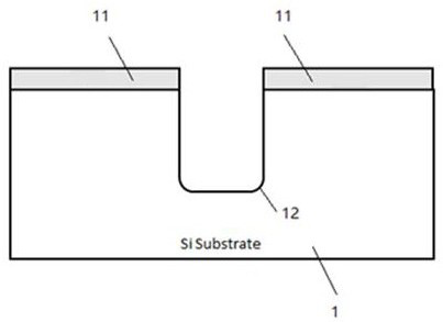
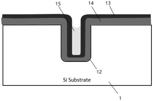
[0034] As shown in the figure, a trench type SGT-MOS device with low leakage and high stability, the epitaxial layer 1 of the device is provided with several trenches 12 built with polycrystalline solid 15; the polycrystalline solid is in the form of I-type structure; the bottom and the inner sidewall of the groove are provided with an insulating layer bonded to the polycrystalline solid; the top of the insulating layer at the inner sidewall of the groove is lower than the epitaxial layer, so that the insulating layer, the epitaxial layer and the sidewall of the polycrystalline solid surround two dielectric grooves 18 located at the sidewall of the I-type polycrystalline solid; the insulating layer is a combined structure including the first insulating structure 13 and the second insulating structure 14 .

[0035] The bottom of the dielectric groove is inclined toward the polycrystalline solid, and is in the shape of a slope or a step with a narrow top and a wide bottom; the di...


PUM


Abstract

The invention provides a trench type SGT-MOS device with low electric leakage and high stability. A plurality of trenches (12) with built-in polycrystalline solids (15) are arranged at an epitaxial layer (1) of the device; the polycrystalline solids are of an I-shaped structure; insulating layers attached to the polycrystalline solids are arranged at the bottom and on the inner side walls of the grooves; the top of an insulating layer at the inner side wall of each groove is lower than the epitaxial layer, so that the insulating layers, the epitaxial layer and the side walls of the polycrystalline solids form two medium grooves (18) at the side walls of the I-type polycrystalline solids; and each insulating layer is a combined structure comprising a first insulating structure (13) and a second insulating structure (14). According to the invention, the problems of non-uniform dielectric thickness, difficult thickness control and large electric leakage of a grid electrode and a source electrode when the dielectric grows in dielectric grooves at the two sides in the device are solved.

Description

technical field [0001] The invention relates to the field of electronic components, in particular to a method for manufacturing a trench type SGT-MOS device with low leakage and high stability. Background technique [0002] Separate gate trench type Mosfet SGT usually adopts a small-scale trench structure (trench width and depth) close to the process limit to make full use of the active area and current path. First, trenches are etched on the epitaxial layer, followed by thermal growth of a certain thickness of silicon dioxide on the sidewalls and bottom of the trenches; doped polysilicon is filled and etched back to the silicon surface at the top of the trenches, and the remaining polysilicon stands on the trenches Between the silicon dioxide in the tank, the shape is similar to the English letter "I". A dielectric tank is made on the left and right sides, filled with polycrystalline and etched back, and finally conductive metal deposition and so on. [0003] However, for ...

Claims


Application Information

Patent Timeline
IPC IPC(8): H01L29/51H01L29/423H01L21/28
CPCH01L29/511H01L29/42368H01L29/4236H01L21/28194H01L21/28185
Inventor 高耿辉苏柳青
Owner 厦门吉顺芯微电子有限公司
Features
  • R&D
  • Intellectual Property
  • Life Sciences
  • Materials
  • Tech Scout
  • Unparalleled Data Quality
  • Higher Quality Content
  • 60% Fewer Hallucinations
Learn More