Aging test device and method for semiconductor storage product

An aging test, semiconductor technology, applied in static memory, instruments, etc., can solve the problems of easy loosening of the test substrate, reduced test accuracy, inconvenience in the fixed positioning of the test substrate, etc., to achieve the effect of simple structure, convenient fixed positioning, and convenient use

Active Publication Date: 2021-08-10
JIANGSU HUACUN ELECTRONICS TECH CO LTD
View PDF5 Cites 3 Cited by
  • Summary
  • Abstract
  • Description
  • Claims
  • Application Information

AI Technical Summary

Problems solved by technology

[0004] The purpose of the present invention is to solve the disadvantages in the prior art that it is inconvenient to fix and position the test substrate during the burn-in test of semiconductor storage products, thus causing the test substrate to be easily loosened and reducing the accuracy of the test. Aging test equipment for semiconductor storage products

Method used


Image

  • Aging test device and method for semiconductor storage product
  • Aging test device and method for semiconductor storage product
  • Aging test device and method for semiconductor storage product

Examples


Embodiment 1

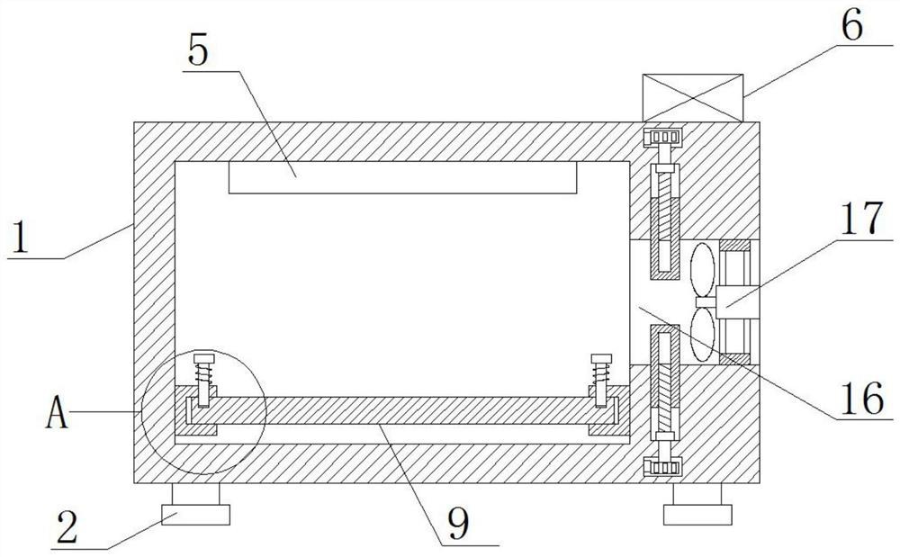
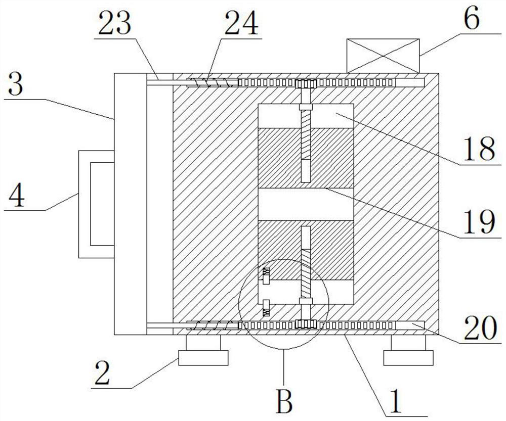
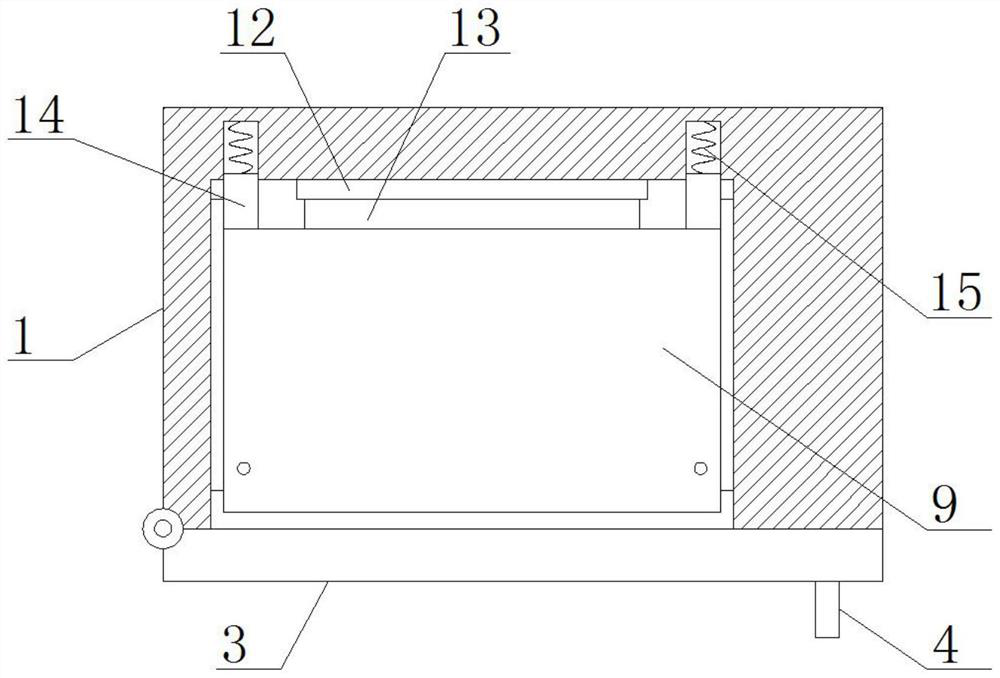
[0031] refer to Figure 1-5 , an aging test device for semiconductor storage products, comprising a box body 1, four fixed feet 2 are fixedly installed on the bottom of the box body 1, a box door 3 is hinged on one side of the box body 1, and a handle is fixedly installed on the box door 3 4. The heating plate 5 is fixedly installed on the inner wall of the top of the box body 1, the power supply 6 is fixedly installed on the top of the box body 1, the inner walls of both sides of the box body 1 are fixedly installed with fixing strips 7, and one side of the two fixing strips 7 is fixed. A first chute 8 is opened, a semiconductor test substrate 9 is slidably installed in the two first chute 8, a plug 13 is fixedly installed on one side of the semiconductor test substrate 9, a socket 12 is fixedly installed on one side of the inner wall of the housing 1, The plug 13 and the socket 12 are snapped together, and one side of the box body 1 is provided with a mounting hole 16, and a...

Embodiment 2

[0039] refer to Figure 1-5 , an aging test device for semiconductor storage products, comprising a box body 1, four fixing feet 2 are fixedly installed on the bottom of the box body 1 by welding, a box door 3 is hinged on one side of the box body 1, and the box door 3 is welded A handle 4 is fixedly installed, a heating plate 5 is fixedly installed on the inner wall of the top of the box body 1 by welding, a power supply 6 is fixedly installed on the top of the box body 1 by welding, and a fixing bar 7 is fixedly installed on both inner walls of the box body 1 by welding One side of the two fixing bars 7 is provided with a first chute 8, a semiconductor test substrate 9 is slidably installed in the two first chute 8, and a plug 13 is fixedly installed on one side of the semiconductor test substrate 9 by welding. The inner wall of one side of the body 1 is fixedly installed with a socket 12 by welding, and the plug 13 and the socket 12 are snapped together. One side of the box...


PUM


Abstract

The invention belongs to the field of semiconductor testing, and particularly relates to an aging test device and method for a semiconductor storage product. Aiming at the problem that a test substrate is easy to loosen and the test accuracy is reduced because the test substrate is inconvenient to fix and position in the process of testing a semiconductor storage product by the existing aging test equipment, the following scheme is provided. The device comprises a box body, four fixing feet are fixedly installed at the bottom of the box body, a box door is hinged to one side of the box body, a handle is fixedly installed on the box door, a heating piece is fixedly installed on the inner wall of the top of the box body, a power source is fixedly installed on the top of the box body, and fixing strips are fixedly installed on the inner walls of the two sides of the box body. According to the invention, the test substrate can be fixed and positioned conveniently in the process of testing the semiconductor storage product, so that the test accuracy reduction caused by the looseness of the test substrate can be prevented. The device is simple in structure and convenient to use.

Description

technical field [0001] The invention relates to the technical field of semiconductor testing, in particular to an aging testing device for semiconductor storage products and a method thereof. Background technique [0002] In order to achieve the qualification rate of semiconductor chips, almost all semiconductor chips are subjected to burn-in tests before leaving the factory. The burn-in test is to provide the necessary system signals for the semiconductor chip to be tested through the semiconductor test board, simulate the working state of the semiconductor chip, accelerate the electrical failure of the semiconductor chip under high temperature or other conditions, and obtain the failure rate of the semiconductor chip within a period of time. Let the semiconductor chip work under a given load state so that the defects appear in a short period of time, so as to obtain the approximate failure rate of the semiconductor chip in the life cycle, and avoid failure in the early sta...

Claims


Application Information

Patent Timeline
Patent Type & Authority Applications(China)
IPC IPC(8): G11C29/56
CPCG11C29/56
Inventor 李庭育庄健民齐元辅
Owner JIANGSU HUACUN ELECTRONICS TECH CO LTD
Why Eureka
Try Eureka