
Optical element surface roughness processing device

A technology of surface roughness and optical components, which is applied in the direction of optical components, optical surface grinders, grinding/polishing safety devices, etc., can solve the problems that the surface roughness cannot be achieved without damage, and achieve the effect of improving the surface roughness

Active Publication Date: 2021-08-17
CHANGCHUN INST OF OPTICS FINE MECHANICS & PHYSICS CHINESE ACAD OF SCI
View PDF14 Cites 2 Cited by
  • Summary
  • Abstract
  • Description
  • Claims
  • Application Information

AI Technical Summary

Problems solved by technology

[0003] In the process of improving roughness, the traditional method is to achieve the marking of the polishing powder in the polishing liquid on the surface of the component through the relative movement of the contact smooth disc and the optical component, thereby improving the surface roughness, but this method will cause damage to the optical component. A sub-surface damage layer was left on the surface, and later a float polishing method was developed, which allowed the element to float on the surface of the polishing disc for relative motion, which solved the problem of the sub-surface damage layer, but this method can only be used for planar optical components, and for spherical surfaces Non-planar surfaces such as , aspheric, and free-form surfaces cannot improve the surface roughness without damage

Method used


Image

  • Optical element surface roughness processing device
  • Optical element surface roughness processing device
  • Optical element surface roughness processing device

Examples


Embodiment Construction

[0030] The following will clearly and completely describe the technical solutions in the embodiments of the present invention with reference to the accompanying drawings in the embodiments of the present invention. Obviously, the described embodiments are only part of the embodiments of the present invention, not all of them. Based on the embodiments of the present invention, all other embodiments obtained by persons of ordinary skill in the art without creative efforts fall within the protection scope of the present invention.

[0031] It should be noted that all directional indications (such as up, down, left, right, front, back...) in the embodiments of the present invention are only used to explain the relationship between the components in a certain posture (as shown in the accompanying drawings). Relative positional relationship, movement conditions, etc., if the specific posture changes, the directional indication will also change accordingly.

[0032] It should also be...


PUM

PropertyMeasurementUnit
Shore hardnessaaaaaaaaaa
elastic modulusaaaaaaaaaa

Abstract

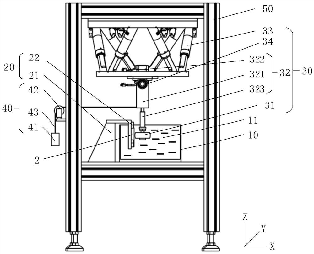
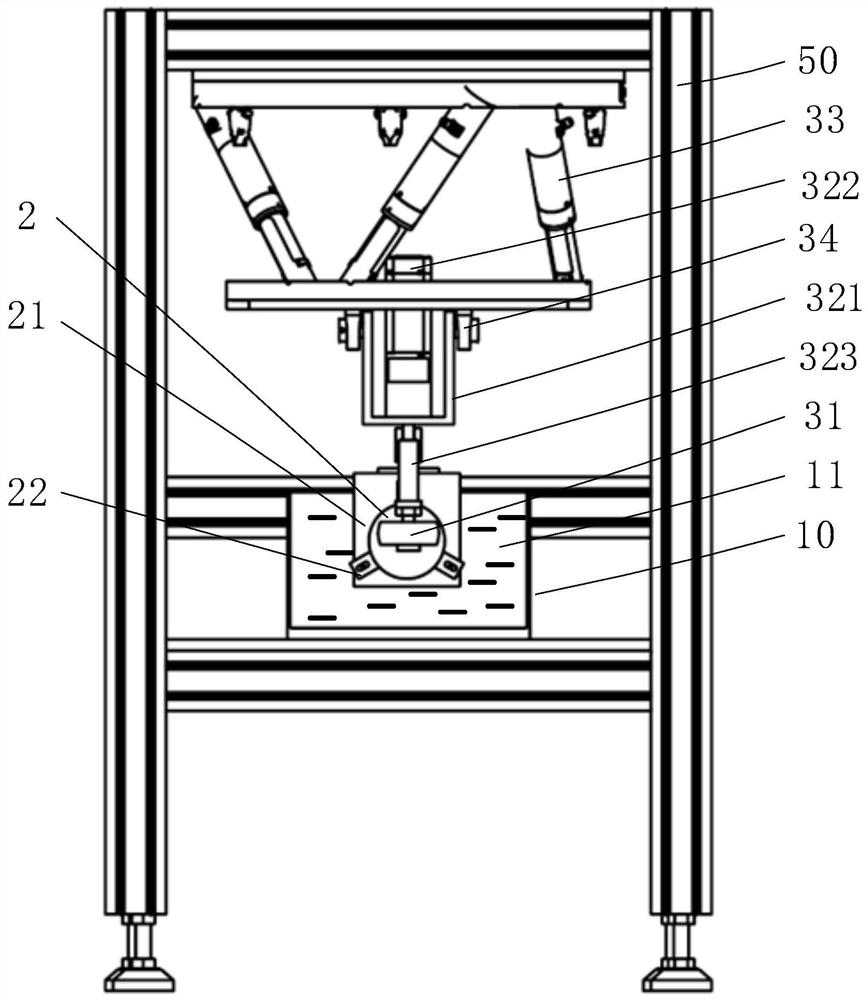
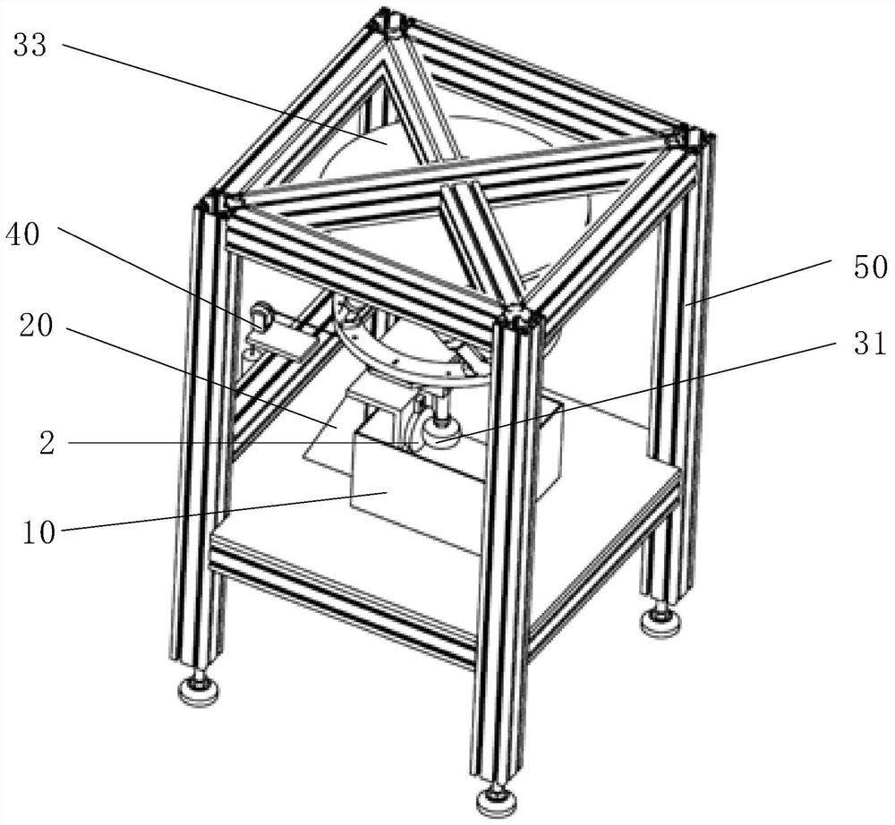
The invention is applicable to the field of optical element processing, and discloses an optical element surface roughness processing device. The optical element surface roughness processing device comprises a storage tank provided with a polishing solution, a bearing assembly for bearing an optical element to be processed, a polishing assembly for processing the surface roughness of the optical element to be processed, and a pressure applying assembly. The polishing assembly comprises a polishing wheel and a first driving mechanism used for driving the polishing wheel to do rotational motion, the hardness and the elastic modulus of the polishing wheel are far lower than those of the optical element to be processed, the pressure applying assembly is used for applying a load close to the optical element to be processed to the polishing wheel, and the polishing wheel and the optical element to be processed are both arranged in the polishing solution. Under the action of the pressure applying assembly, the contact part of the polishing wheel and the optical element to be processed can deform, a liquid film is formed between the deformation part of the polishing wheel and the optical element to be processed, so that non-contact polishing is performed between the polishing wheel and the optical element to be processed, and the surface roughness of the optical element can be improved; and the surface of the optical element to be processed has no sub-surface damage.

Description

technical field [0001] The invention relates to the technical field of optical element processing, in particular to a device capable of processing the surface roughness of optical elements on a plane, a spherical surface, an aspheric surface or a free-form surface. Background technique [0002] In the field of high-precision optical processing, the transmissive or reflective optical elements in the optical system generally include flat mirrors, spherical mirrors, aspheric mirrors, and free-form mirrors. degrees and other stages. With the precision optical system, the precision of the optical components is getting higher and higher, especially the roughness of the surface of the optical components is getting higher and higher, and in special applications, the optical components are also required to be free of subsurface damage. [0003] In the process of improving the roughness, the traditional way is to achieve the marking of the polishing powder in the polishing liquid on ...

Claims


Application Information

Patent Timeline
Patent Type & Authority Applications(China)
IPC IPC(8): B24B13/00B24B13/005B24B27/00B24B55/02B24B41/02
CPCB24B13/00B24B13/0055B24B27/0015B24B55/02B24B41/02
Inventor 郭本银张海涛金春水
Owner CHANGCHUN INST OF OPTICS FINE MECHANICS & PHYSICS CHINESE ACAD OF SCI
Learn More