Eureka AIR delivers breakthrough ideas for toughest innovation challenges, trusted by R&D personnel around the world.

Graphite substrate and manufacturing method thereof

A technology for a graphite substrate and a manufacturing method, which is applied to chemical instruments and methods, crystal growth, and chemically reactive gases, etc., can solve the problems such as the short wavelength of the edge of the graphite substrate, affecting the distribution of Mo source gas, and aggravating the flow rate of the MO source gas flow, etc. , to achieve the same luminous wavelength, improve the flow rate too fast, improve the uniformity of the chip

Active Publication Date: 2022-04-15
HC SEMITEK ZHEJIANG CO LTD
View PDF0 Cites 0 Cited by
  • Summary
  • Abstract
  • Description
  • Claims
  • Application Information

AI Technical Summary

Problems solved by technology

[0005] The graphite substrate rotates at high speed during the formation of the epitaxial wafer, and there is gas flow on the surface of the graphite substrate at high speed, which will affect the gas distribution of the Mo source in the reaction chamber during the growth of the epitaxial wafer
And the farther away from the center of the graphite substrate, the distribution of the MO source will appear uneven
In particular, the edge position of the graphite substrate is subject to the largest centrifugal force and the largest linear velocity, which will intensify the flow velocity of the MO source gas flow, resulting in the phenomenon that the edge wavelength of the graphite substrate is abnormally short or long.

Method used


Image

  • Graphite substrate and manufacturing method thereof
  • Graphite substrate and manufacturing method thereof
  • Graphite substrate and manufacturing method thereof

Examples


Embodiment Construction

[0030] In order to make the purpose, technical solution and advantages of the present disclosure clearer, the implementation manners of the present disclosure will be further described in detail below in conjunction with the accompanying drawings.

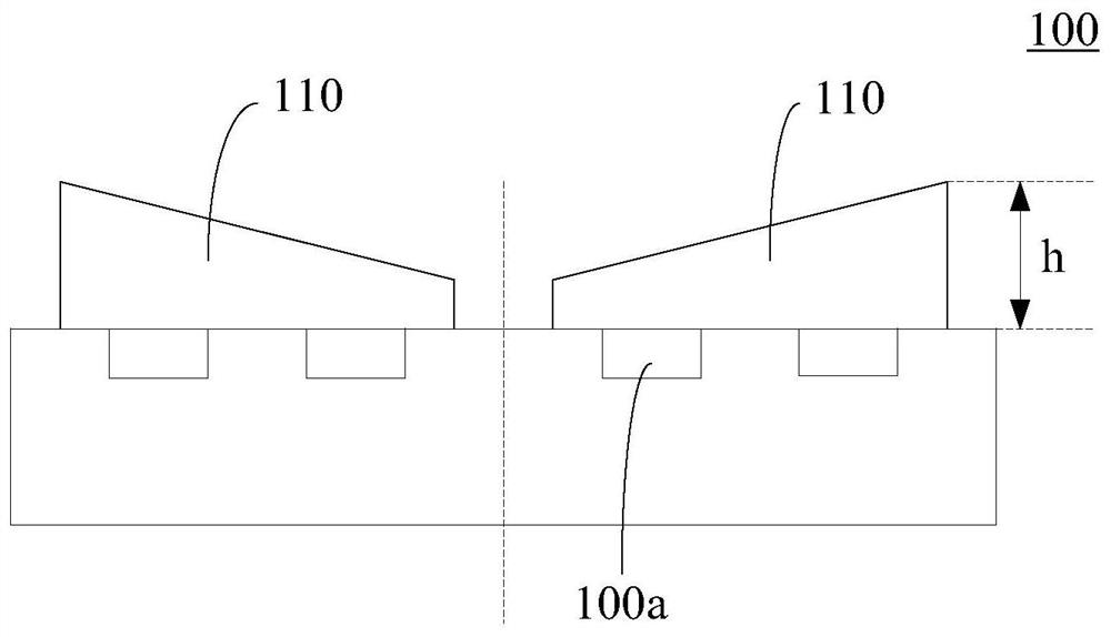
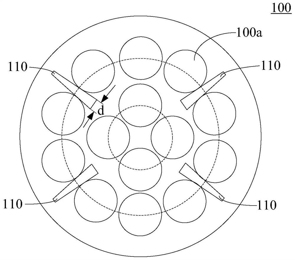
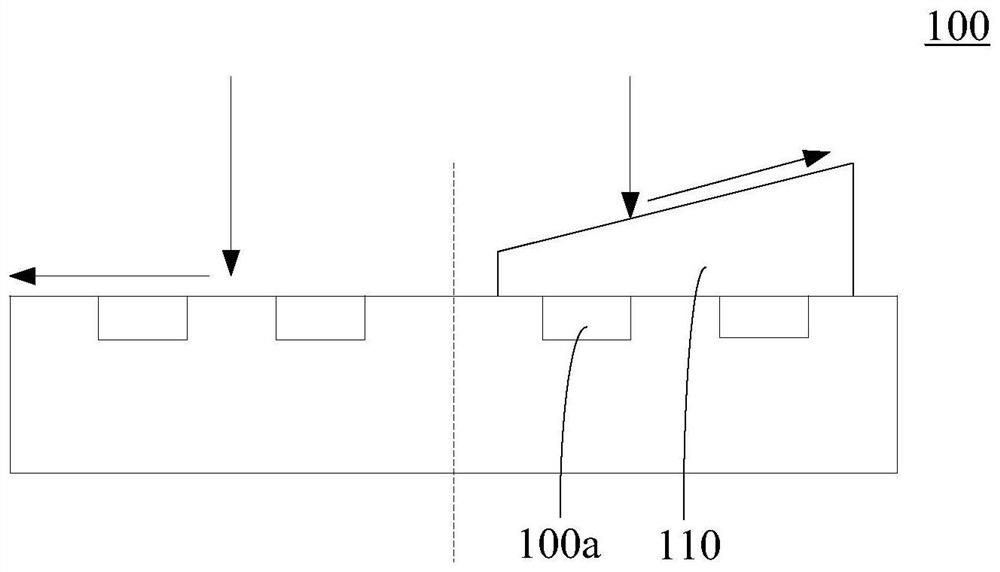
[0031] figure 1 is a front view of a graphite substrate provided by an embodiment of the present disclosure, figure 2 is a top view of a graphite substrate provided by an embodiment of the present disclosure, such as figure 1 and figure 2 As shown, the graphite substrate 100 is a disc, and the first surface of the graphite substrate 100 has multiple rings of grooves 100a for accommodating the substrate. The multiple rings of grooves 100 a are coaxial with the graphite substrate 100 , and each ring of grooves 100 a includes a plurality of grooves.

[0032] The graphite substrate 100 also includes a plurality of protruding structures 110 arranged on the first surface of the graphite substrate 100 in the radial direction of the g...


PUM


Abstract

The disclosure provides a graphite substrate and a manufacturing method thereof, belonging to the technical field of semiconductors. The first surface of the graphite substrate has multiple turns of grooves for accommodating the substrate, the multiple turns of grooves are all coaxial with the graphite substrate, and each turn of the grooves includes a plurality of grooves; The graphite substrate also includes a plurality of protruding structures arranged on the first surface of the graphite substrate along the radial direction of the graphite substrate, and the plurality of protruding structures are located in the plurality of the multi-circle grooves. Between the grooves, and from the center of the graphite substrate to the edge of the graphite substrate, the height of the raised structure gradually increases. The growth of the epitaxial wafer on the graphite substrate provided by the present disclosure can make the emission wavelength of each region of the epitaxial wafer consistent, thereby improving the uniformity of the epitaxial wafer and ensuring the edge yield.

Description

technical field [0001] The present disclosure relates to the technical field of semiconductors, in particular to a graphite substrate and a manufacturing method thereof. Background technique [0002] A semiconductor light-emitting diode (English: Light Emitting Diode, referred to as: LED) is a semiconductor diode that can convert electrical energy into light energy. LED has the advantages of high efficiency, energy saving, and environmental protection, and is widely used in traffic indication, outdoor full-color display and other fields. In particular, the use of high-power LEDs to realize semiconductor solid-state lighting is expected to become a new generation of light sources and enter thousands of households, causing a revolution in the history of human lighting. [0003] The epitaxial wafer is the primary product in the LED manufacturing process. When forming an epitaxial wafer, the substrate is placed on a tray in the reaction chamber of a metal organic chemical vapo...

Claims


Application Information

Patent Timeline
Patent Type & Authority Patents(China)
IPC IPC(8): C30B25/14C30B25/18C23C16/458C23C16/455H01J37/32
CPCC30B25/18C30B25/14C23C16/4585C23C16/45591H01J37/32449H01J37/32715
Inventor 葛永晖梅劲刘春杨丁涛陈张笑雄王慧
Owner HC SEMITEK ZHEJIANG CO LTD
Why Eureka
Eureka Blog
Learn More