Manufacturing method of thick gas electronic multiplication detector diaphragm board

A technology of gas electron multiplication and production method, which is applied in the direction of removing conductive materials by chemical/electrolytic methods, can solve problems such as affecting the working performance of the detector, increasing the difficulty of making the THGEM membrane, and achieve the effect of uniformity and uniformity.

Active Publication Date: 2014-03-12
UNIVERSITY OF CHINESE ACADEMY OF SCIENCES +1
View PDF5 Cites 16 Cited by
  • Summary
  • Abstract
  • Description
  • Claims
  • Application Information

AI Technical Summary

Problems solved by technology

Among them, the most difficult to control is the lamination process. Since the lamination needs to be aligned with the center of each hole, otherwise the performance of the detector will be affected due to the poor quality of a single hole. Therefore, the exis

Method used


Image

  • Manufacturing method of thick gas electronic multiplication detector diaphragm board
  • Manufacturing method of thick gas electronic multiplication detector diaphragm board
  • Manufacturing method of thick gas electronic multiplication detector diaphragm board

Examples


Example Embodiment

[0031] Example 1

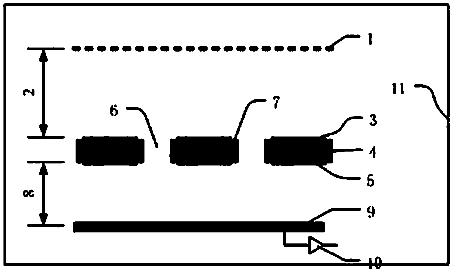
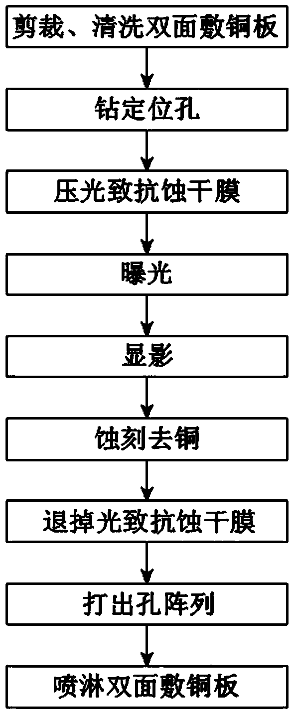
[0032] 1. Cut the double-sided copper-clad PCB board into a production board with a processing size of 300mm×300mm, scrub and clean it with a board brushing machine, and use a cleaning agent to remove grease, etc., and wait for use.

[0033] 2. Drill positioning holes on the double-sided copper clad board for the installation and fixing of THGEM membrane board.

[0034] 3. Simultaneously press the photoresist dry film on both sides of the double-sided copper clad board.

[0035] 4. Align the outer graphics film with the circuit board with the photoresist dry film pressed, put it on the exposure machine for exposure, and bake at 100°C for 3 minutes.

[0036] 5. Use NaCO with a concentration of 1% (w / v) 3 The solution was developed at a spray speed of 0.8m / min.

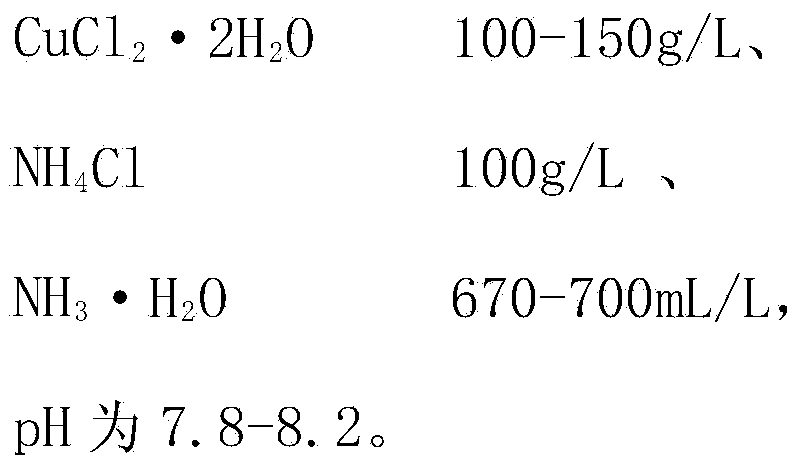
[0037] 6. Etch copper with etching solution, the composition of etching solution is:

[0038]

[0039] 7. Remove the photoresist dry film with film removing solution. At this time, the upper l...

Example Embodiment

[0045] Example 2

[0046] 1. Cut the double-sided copper-clad PCB board into a production board with a processing size of 300mm×300mm, scrub and clean it with a board brushing machine, and use a cleaning agent to remove grease, etc., and wait for use.

[0047] 2. Drill positioning holes on the double-sided copper clad board for the installation and fixing of THGEM membrane board.

[0048] 3. Simultaneously press the photoresist dry film on both sides of the double-sided copper clad board.

[0049] 4. Align the outer graphics film with the circuit board with the photoresist dry film pressed, put it on the exposure machine for exposure, and bake at 100°C for 3 minutes.

[0050] 5. Use NaCO with a concentration of 1% (w / v) 3 The solution was developed at a spray speed of 0.8m / min.

[0051] 6. Etch copper with etching solution, the composition of etching solution is:

[0052]

[0053] 7. Remove the photoresist dry film with film removing solution. At this time, the upper l...


PUM


Abstract

The invention discloses a manufacturing method of a thick gas electronic multiplication detector diaphragm board. The method is characterized by including: cutting and cleaning a board clad with copper on two sides; drilling positioning holes; simultaneously pressing light-induced anti-corrosion dry diaphragms on two sides; aligning an external pattern film with the circuit board with the light-induced anti-corrosion dry diaphragms, and exposing the two on an exposure machine; developing and etching to remove copper and the light-induced anti-corrosion dry diaphragms; using a numerical control machine tool to punch hole arrays on the board clad with copper on two sides; spraying the board clad with copper on two sides. The method has the advantages that entire board micro-etching is used for manufacturing, manufacturing of large-area THGEM diaphragm boards is facilitated, the 300*300mm THGEM diaphragm boards is manufactured successfully, and rim uniformity is consistent; full-automatic circuit board manufacturing equipment is used, batch production can be achieved, and yield can reach more than 95%; the THGEM diaphragm boards are independent of reading anode plates and can be designed and machined into different sizes and shapes according to needs.

Description

technical field [0001] The invention relates to a method for manufacturing a diaphragm, in particular to a method for manufacturing a thick gas electron multiplication detector diaphragm, which belongs to the field of etching processing. Background technique [0002] Thick gas electron multiplier detector (THGEM) is a new type of microstructured gas detector, its structure is as follows: figure 1 As shown, in the airtight chamber 11 (the airtight chamber 11 is filled with working gas, which can be mixed with inert gases such as argon and xenon and quenching gases such as carbon dioxide, isobutane and methane), the drift electrode 1 , the readout anode 9 and the preamplifier 10 are arranged parallel to each other, and a THGEM diaphragm is also arranged in parallel between the drift electrode 1 and the readout anode 9. The THGEM diaphragm is composed of an upper copper layer 3, an insulating substrate 4 and a lower copper layer. 5, the THGEM film plate is provided with an arr...

Claims


Application Information

Patent Timeline
IPC IPC(8): H05K3/06
Inventor 郑阳恒刘宏邦刘倩谢一冈陈石周晓康董洋张强李雪冰张炜汪晶常洁
Owner UNIVERSITY OF CHINESE ACADEMY OF SCIENCES
Why Eureka
Try Eureka