Check patentability & draft patents in minutes with Patsnap Eureka AI!

Array substrate and display panel

An array substrate and plate technology, applied in nonlinear optics, instruments, optics, etc., can solve the problems of lower pixel penetration rate, lower production yield, and poor alignment, so as to increase pixel aperture ratio and improve electric current. Sexual stability, improve the effect of large-screen role bias

Pending Publication Date: 2021-08-27
TCL CHINA STAR OPTOELECTRONICS TECH CO LTD
View PDF0 Cites 8 Cited by
  • Summary
  • Abstract
  • Description
  • Claims
  • Application Information

AI Technical Summary

Problems solved by technology

[0004] However, this pixel design is connected to the preset electrode (sharebar) electrode through the drain of the third thin film transistor. The preset electrode is located under the pixel electrode (ITO) trunk. Poor alignment between the preset electrode and the pixel electrode will reduce the pixel transmittance. , at the same time, foreign matter between the default electrode and the underlying common electrode metal may cause poor light lines, resulting in a decline in production yield

Method used


Image

  • Array substrate and display panel
  • Array substrate and display panel
  • Array substrate and display panel

Examples


Embodiment 1

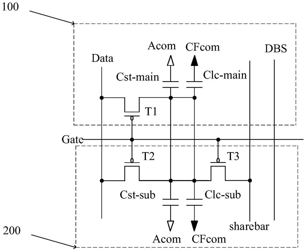
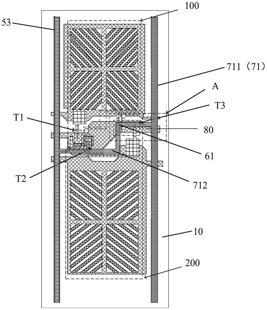
[0042] see figure 2 , a top view of the sub-pixels of the array substrate provided by the embodiment of the present application.

[0043] This embodiment provides an array substrate, and the array substrate includes a plurality of scanning lines 80 extending in the horizontal direction, a plurality of data lines 53 extending in the vertical direction, and a plurality of non-black lines located above the plurality of data lines 53. The data lines 71 of the matrix and a plurality of sub-pixels defined by intersections of the scan lines 80 and the data lines 53 .

[0044] Each sub-pixel is divided into a main pixel area 100 and a sub-pixel area 200, and a scanning line 80 is provided corresponding to each row of the sub-pixels, and the scanning line 80 is between the main pixel area 100 and the sub-pixel Between area 200.

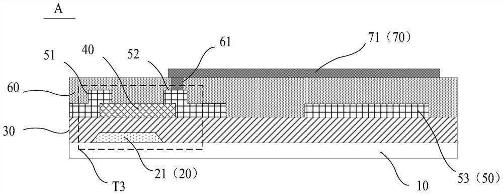
[0045] The main pixel area 100 of the sub-pixel includes a first thin film transistor T1, a main area storage capacitor Cst-main, and a main area liquid cr...

Embodiment 2

[0059] This embodiment also provides a display panel, including the array substrate as described in any one item.


PUM


Abstract

The invention provides an array substrate and a display panel. The array substrate comprises a plurality of scanning lines, a plurality of data lines, a plurality of data lines without black matrixes and a plurality of sub-pixels, wherein the data lines are located above the data lines, and the sub-pixels are defined by the scanning lines and the data lines in a crossed mode. Each sub-pixel is divided into a main pixel area and an auxiliary pixel area, a scanning line is arranged corresponding to each row of sub-pixels, and the scanning lines are located between the main pixel areas and the auxiliary pixel areas; the main pixel area comprises a first thin film transistor, a main area storage capacitor and a main area liquid crystal capacitor, and the auxiliary pixel area comprises a second thin film transistor, a third thin film transistor, an auxiliary area storage capacitor and an auxiliary area liquid crystal capacitor; wherein the drain electrode of the third thin film transistor is connected with the data line of the non-black matrix, so that the pixel aperture opening ratio is increased, meanwhile, a preset electrode is omitted, and the occurrence probability of poor pixels can be effectively reduced.

Description

technical field [0001] The present application relates to the field of display technology, and in particular to an array substrate and a display panel. Background technique [0002] In the 3T pixel unit structure, the pixel unit is divided into a main pixel area (Main Pixel) and a sub-pixel area (SubPixel). In the prior art, the problem of viewing angle is improved through the different degrees of liquid crystal inversion in the main pixel area and the sub-pixel area. [0003] The main pixel area is driven by a first thin film transistor (Thin Film Transistor, TFT), and the sub-pixel area is jointly driven by a second thin film transistor and a third thin film transistor for pulling down the voltage of the sub-pixel area. Wherein, the gate of the first thin film transistor in the main pixel area is connected to the corresponding scanning line Gate, the source of the first thin film transistor is connected to the corresponding data line Data, and the drain of the first thin f...

Claims


Application Information

Patent Timeline
IPC IPC(8): G02F1/1362G02F1/1368
CPCG02F1/13624G02F1/1368
Inventor 杨光陈亚妮
Owner TCL CHINA STAR OPTOELECTRONICS TECH CO LTD
Features
  • R&D
  • Intellectual Property
  • Life Sciences
  • Materials
  • Tech Scout
  • Unparalleled Data Quality
  • Higher Quality Content
  • 60% Fewer Hallucinations
Learn More