Normal/flip MiniLED display panel capable of improving display effect and preparation method thereof

A display effect and display panel technology, which is applied in the direction of identification devices, instruments, electrical components, etc., can solve the problem that the contrast ratio of small-pitch products cannot be larger, the area of ​​bonding pads cannot be small, and the brightness of LED light-emitting chips is not high. Advanced problems, to achieve the effect of saving labor hours, improving display effects, and meeting market needs

Inactive Publication Date: 2021-08-27
吴越
View PDF0 Cites 1 Cited by
  • Summary
  • Abstract
  • Description
  • Claims
  • Application Information

AI Technical Summary

Problems solved by technology

However, it is limited because the COB packaging must consider the bonding pad and the bonding pad, and because the bonding area is too large, the bonding pad area cannot be made very small, and the brightness of the vertically packaged LED light-emitting chip is not high. Several reasons lead to COB packaging small pitch products can not achieve greater contrast
Moreover, the existing COB display panels face technical bottlenecks such as poor ink color consistency, poor flatness, high cost, and difficult maintenance.

Method used


Image

  • Normal/flip MiniLED display panel capable of improving display effect and preparation method thereof
  • Normal/flip MiniLED display panel capable of improving display effect and preparation method thereof
  • Normal/flip MiniLED display panel capable of improving display effect and preparation method thereof

Examples


Embodiment Construction

[0033] In order to make the technical means realized by the present invention, creative features, goals and effects easy to understand, the present invention will be further elaborated below in conjunction with specific embodiments.

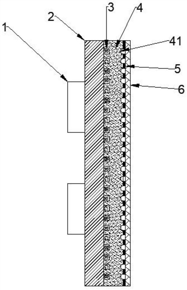
[0034] refer to figure 1 , Fig. 2(a), Fig. 2(b) and Fig. 2(c), the present embodiment adopts the following technical scheme: a front-side flip-chip Mini LED display panel to improve the display effect, including a driver IC1, a driver circuit board 2, a spatial structure Pixel unit 3, encapsulation adhesive layer 4, black encapsulation formula layer 5 and surface optical treatment layer 6, the drive IC1 adopts a high-brush chip with precise voltage control, and the drive IC1 is arranged on one side of the drive circuit board 2, and the drive circuit board 2 The other side is provided with a spatial structure pixel unit (3), the outer side of the spatial structure pixel unit 3 is provided with a packaging adhesive layer 4, the outer packaging adhe...


PUM


Abstract

The invention discloses a normal/flip MiniLED display panel capable of improving the display effect and a preparation method thereof, and relates to the technical field of LED display screens. The normal/flip MiniLED display panel comprises a driving IC, a driving circuit board, a spatial structure pixel unit, a packaging glue layer, a black packaging formula layer and a surface optical processing layer. The driving IC adopts a high-brush chip with precise voltage control, the driving IC is arranged on one side of the driving circuit board, the spatial structure pixel unit is arranged on the other side of the driving circuit board, the packaging glue layer is arranged on the outer side of the spatial structure pixel unit, the black packaging formula layer is arranged outside the packaging glue layer, and the surface optical processing layer is arranged on the outer side of the black packaging formula layer. The manufacturing process is simple, the cost is ultra-low, the performance is optimal, the batch production yield is high, maintenance can be achieved, the service life is long, and the product can be improved along with the market; and any requirements of the market can be met only by updating software without changing hardware, and iteration and updating of the product are formed.

Description

technical field [0001] The invention relates to the technical field of LED display screens, in particular to a flip-chip Mini LED display panel with improved display effect and a preparation method thereof. Background technique [0002] With the development of small-pitch COB packaging technology, COB small-pitch packaging products have gradually become a hot spot. The main reason is that compared with the current mainstream surface-mount technology, COB small-pitch integrated packaging can achieve smaller dot pitches. The technical advantages of COB small-pitch products mainly include two points: first, the adhesive layer on the surface of COB small-pitch products is more conducive to protecting the light-emitting surface; The field of small spacing has natural technical advantages. The technical route of COB integrated small-pitch packaging is to place the chip directly on the PCB, the flip-chip product is connected to the PCB through solder paste, and the front-mounted p...

Claims


Application Information

Patent Timeline
Patent Type & Authority Applications(China)
IPC IPC(8): H01L33/56H01L25/075H01L33/58G09F9/33
CPCG09F9/33H01L25/0753H01L33/56H01L33/58H01L2933/0033
Inventor 吴越
Owner 吴越
Why Eureka
Try Eureka