Embedded synthetic network substrate lamination based on multiple lamination and design method

A technology of multiple lamination and design methods, applied in the direction of multi-layer circuit manufacturing, printed circuits, electrical components, etc., can solve the problem of difficult to meet the needs of high-density integrated applications, and achieve flexible and convenient application, convenient wiring, and RF signal isolation. good performance

Active Publication Date: 2021-08-27
SOUTHWEST CHINA RES INST OF ELECTRONICS EQUIP
View PDF12 Cites 0 Cited by
  • Summary
  • Abstract
  • Description
  • Claims
  • Application Information

AI Technical Summary

Problems solved by technology

At present, the beamforming network of broadband board-level integration is limited by the stacking of the substrate. The large-sized beamforming network is realized through radio frequency package integration or a small amount of internal embedding, which is difficult to meet the current application requirements of high-density integration. Continue to design A radio frequency substrate stackup suitable for array synthesis network

Method used


Image

  • Embedded synthetic network substrate lamination based on multiple lamination and design method
  • Embedded synthetic network substrate lamination based on multiple lamination and design method
  • Embedded synthetic network substrate lamination based on multiple lamination and design method

Examples


Embodiment 1

[0035] This embodiment provides a multi-lamination-based design method for embedded synthetic network substrate stacking, including: laminating one radio frequency layer and two ground property layers into a basic unit, wherein , the radio frequency layer is located in the middle of the two ground property layers;

[0036] A single basic unit is stacked as an array composite network integrated substrate or multiple basic units are laminated multiple times, and at the same time, a radio frequency isolation hole that conducts the entire basic unit is separately designed in the basic unit.

[0037] Specifically, in this embodiment, as figure 1 As shown, a single basic unit is used as an array composite network substrate stack, and the radio frequency layer in the basic unit is placed between the two ground property layers in the way of embedded resistance film processing, so as to realize the corresponding coupling and board-level embedding of the composite network. The size of ...

Embodiment 2

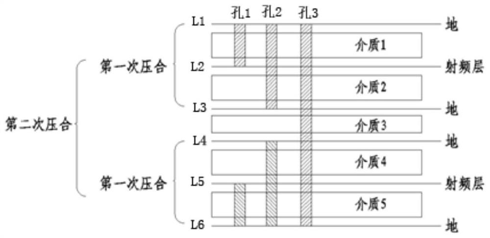
[0042] This embodiment is basically the same as Embodiment 1, the difference is that in this embodiment, the array synthesis network integrated substrate stack is composed of two basic units, when the array synthesis network integrated substrate stack is composed of multiple basic units When the unit is formed, a plurality of basic units are provided with communicating ground holes or installation holes.

[0043] Such as figure 2 As shown, the two basic unit structures are laminated twice to form an array composite network integrated substrate stack, in which L2 and L5 are two radio frequency layers, and the upper and lower layers (L1, L3, L4, L6) are ground Attribute layer, each layer has an independent radio frequency isolation hole (hole 2), which is used for signal isolation and electromagnetic shielding around the grounding and radio frequency transmission lines. Hole 1 is the gap between the L2, L5 radio frequency layer and the respective surface layers L1, L6 Signal t...

Embodiment 3

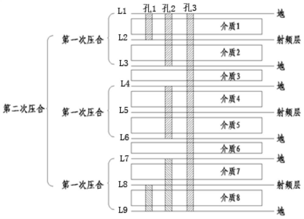
[0048] This embodiment is basically the same as Embodiment 1 and Embodiment 2, the difference is that in this embodiment, the array synthesis network integrated substrate stack is composed of three basic units, such as image 3 As shown, the laminated structure formed by secondary pressing of three basic unit structures, in which L2, L5, and L8 are three radio frequency layers, each of which has two upper and lower layers (L1, L3, L4, L6, L7, L9) They are all ground layers, and each layer has an independent radio frequency shielding hole (hole 2), which is used for signal isolation and electromagnetic shielding around the grounding and radio frequency transmission lines. Hole 1 is for the L2, L8 radio frequency transmission layer and the respective surface layers L1, The signal transmission hole between L9, hole 3 can be used as a ground hole, installation hole, etc. Arbitrary layer interconnection of radio frequency signals and addition of low frequency layers can be designed...


PUM


Abstract

The invention relates to the field of radio frequency circuits, and discloses an embedded synthetic network substrate lamination based on multiple lamination and a design method. An array synthetic network integrated substrate lamination provided by the present invention comprises a plurality of base units which are laminated together, each base unit comprises two ground attribute layers and a radio frequency layer, and the radio frequency layer is arranged between the two ground attribute layers in an embedded resistive film processing manner. At least two ground attribute layers and one digital / power supply control layer are arranged between the adjacent radio frequency layers, each basic unit is independently provided with a radio frequency isolation hole, the basic units at the two ends are further provided with radio frequency signal transmission holes used for transmitting radio frequency signals, and communicated ground holes or mounting holes are formed between the multiple basic units which are laminated together. The array synthetic network integrated substrate lamination provided by the invention has the advantages of various lamination combination modes, flexible design, flexible and convenient application and very good radio frequency signal isolation performance, and can realize the very high radio frequency isolation requirements.

Description

technical field [0001] The invention relates to the field of radio frequency circuits, in particular to the technical field of wideband phased array front-end and synthetic network design, specifically a multi-lamination-based embedded synthetic network substrate lamination and design method. Background technique [0002] With the rapid development of radar, communication and other systems, phased array systems are more and more used in various radar and communication systems, and in phased array systems, the array synthesis network is its main part, its performance and size Has a very large impact on the performance and size of the array system. As the low-profile requirements of the array system become more and more urgent, how to design an array synthesis network with excellent performance and small size (especially in the cross-sectional direction) becomes more and more important. [0003] The implementation methods of the array synthesis network of the phased array sys...

Claims


Application Information

Patent Timeline
Patent Type & Authority Applications(China)
IPC IPC(8): H05K3/46
CPCH05K3/4623H05K2203/061H05K2203/068
Inventor 笪余生周俊杜顺勇高阳马磊强杨非宋阳罗洋
Owner SOUTHWEST CHINA RES INST OF ELECTRONICS EQUIP
Why Eureka
Try Eureka