A kind of non-solder package embedded in bga chip for hybrid package

A hybrid packaging, no soldering technology, applied in the direction of electrical components, electrical solid devices, circuits, etc., can solve problems such as solder joints, affecting product quality, and air in packaging, to achieve short circuit between, good compatibility, and reduce Effect of Small Thickness and Volume

Inactive Publication Date: 2016-10-05
NO 8357 RES INST OF THE THIRD ACADEMY OF CHINA AEROSPACE SCI & IND
View PDF5 Cites 0 Cited by
  • Summary
  • Abstract
  • Description
  • Claims
  • Application Information

AI Technical Summary

Problems solved by technology

For BGA chips mixed with traditional technology, there are problems such as solder joints and air in the package, which seriously affect product quality.

Method used


Image

  • A kind of non-solder package embedded in bga chip for hybrid package
  • A kind of non-solder package embedded in bga chip for hybrid package
  • A kind of non-solder package embedded in bga chip for hybrid package

Examples


Embodiment 1

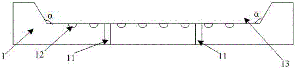
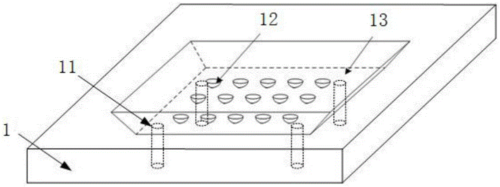
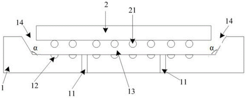
[0028] The present embodiment adopts the BGA chip 2 of 7 * 7mm, and the diameter of the BGA solder ball 21 on the BGA chip is 0.25mm, and the size of the organic substrate mounting cavity 13 that matches this is 7 * 7mm, and the four dimensions of the mounting cavity 13 Both sides are isosceles trapezoidal slopes, the angle α between the isosceles trapezoidal slopes and the bottom surface of the installation cavity is 105°, the depth of the installation cavity 13 is 1 / 6 of the thickness of the organic substrate 1, and the bottom surface of the organic substrate is provided with 2 through holes 11, and the through holes are evenly and symmetrically distributed, the diameter of the hemispherical groove 12 on the bottom surface of the installation cavity is 0.25mm, and the inner surface of the hemispherical groove 12 is plated with a metal tin layer.

Embodiment 2

[0030] The present embodiment adopts the BGA chip 2 of 15 * 15mm, the diameter of the BGA solder ball 21 on the BGA chip is 0.5mm, and the size of the organic substrate mounting cavity 13 that matches this is 15 * 15mm, and the mounting cavity 13 is symmetrical Both sides are isosceles trapezoidal slopes, the angle α between the isosceles trapezoidal slopes and the bottom surface of the installation cavity is 115°, the depth of the installation cavity 13 is 1 / 3 of the thickness of the organic substrate 1, and the bottom surface of the organic substrate is provided with 6 through holes. Holes 11, and the through holes are evenly and symmetrically distributed, the diameter of the hemispherical groove 12 on the bottom surface of the installation cavity is 0.5mm, and the inner surface of the hemispherical groove 12 is plated with a metal tin layer.

Embodiment 3

[0032]The present embodiment adopts the BGA chip 2 of 20 * 20mm, the diameter of the BGA solder ball 21 on the BGA chip is 1mm, and the size of the organic substrate mounting cavity 13 that matches this is 20 * 20mm, and the four sides of the mounting cavity 13 They are all isosceles trapezoidal slopes, the angle α between the isosceles trapezoidal slopes and the bottom surface of the installation cavity is 130°, the depth of the installation cavity is 1 / 2 of the thickness of the organic substrate, and the bottom surface of the organic substrate is provided with 12 through holes 11, and through The holes are evenly and symmetrically distributed, and the diameter of the hemispherical groove 12 on the bottom surface of the installation cavity is 1mm, and the inner surface of the hemispherical groove 12 is plated with a metal tin layer.


PUM


Abstract

The invention relates to a solderless package embedded with a BGA chip for hybrid packaging, which is characterized in that the package includes an organic substrate, and an installation cavity matching the BGA chip is arranged in the center of the upper part of the organic substrate, and the installation cavity is a rib Table shape, at least one side is an isosceles trapezoidal slope, the angle between the isosceles trapezoidal slope and the bottom surface of the installation cavity is 105-130°, after the BGA chip is placed in the installation cavity, at least one side has a plastic encapsulation inlet, and the installation The depth of the cavity is 1 / 6-1 / 2 of the thickness of the organic substrate, and the bottom surface of the installation cavity is provided with hemispherical grooves. matching, and the inner surface of the hemispherical groove is coated with a metal layer; the bottom surface of the organic substrate is evenly distributed with 4-6 through holes for vacuuming per square centimeter.

Description

technical field [0001] The invention relates to semiconductor packaging technology, in particular to a non-soldering packaging used for embedded BGA chips in hybrid packaging. Background technique [0002] System-in-a-Package (SiP for short) mainly uses 3D packaging technology to put various chip original chips with complete system functions into a chip package to realize the integration of system functions and the reduction of volume and weight. Technology, 3D packaging technology, substrate, package design, processing and manufacturing technology and other advanced design and processing technologies are highly cross-integrated products. In SiP, chips, bare chips, passive devices, etc. can be used for hybrid packaging to achieve more system functions, more flexibility, and low cost. [0003] The development of hybrid packaging has a history of many years, and the application of hybrid packaging technology can be seen from the earliest component-level products to the curren...

Claims


Application Information

Patent Timeline
Patent Type & Authority Patents(China)
IPC IPC(8): H01L23/31H01L23/13H01L21/56
Inventor 朱天成李鑫杨阳
Owner NO 8357 RES INST OF THE THIRD ACADEMY OF CHINA AEROSPACE SCI & IND
Why Eureka
Try Eureka