
Damping device and method for in-situ deformation of micro-nano sample in microscope

A shock-absorbing device, microscope technology, applied in measurement devices, material analysis using radiation diffraction, testing material strength using applied stable tension/pressure, etc. The problems of large chip spacing and too many hanging nets can save time and price costs, be easy to fix, and have fewer preparation steps.

Pending Publication Date: 2021-08-31
BEIJING UNIV OF TECH
View PDF6 Cites 0 Cited by
  • Summary
  • Abstract
  • Description
  • Claims
  • Application Information

AI Technical Summary

Problems solved by technology

The device can realize the stretching experiment of one-dimensional nanowires, but due to technical limitations, the distance between the two bimetallic sheets glued to the metal ring is relatively large (more than 50 μm), which makes the carrier grid of the micro-nano material suspended in the air. More, it is easy to cause the sample to break during the transfer and loading process, making it difficult to achieve stable stretching and atomic-scale observation

Method used


Image

  • Damping device and method for in-situ deformation of micro-nano sample in microscope
  • Damping device and method for in-situ deformation of micro-nano sample in microscope
  • Damping device and method for in-situ deformation of micro-nano sample in microscope

Examples


Embodiment Construction

[0028] The following will clearly and completely describe the technical solutions in the embodiments of the present invention with reference to the accompanying drawings in the embodiments of the present invention. Obviously, the described embodiments are only some, not all, embodiments of the present invention. Based on the embodiments of the present invention, all other embodiments obtained by persons of ordinary skill in the art without making creative efforts belong to the protection scope of the present invention.

[0029] In order to make the above objects, features and advantages of the present invention more comprehensible, the present invention will be further described in detail below in conjunction with the accompanying drawings and specific embodiments.

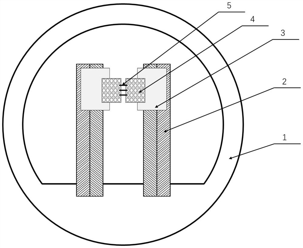
[0030] The present invention provides a shock absorbing device for deforming micro-nano samples in situ in a microscope, including a support part 1, a power part 2, a shock absorbing part 3 and a grid 4; the suppor...


PUM

PropertyMeasurementUnit
thicknessaaaaaaaaaa
lengthaaaaaaaaaa
lengthaaaaaaaaaa

Abstract

The invention discloses a damping device and method for in-situ deformation of a micro-nano sample in a microscope, belonging to the field of measurement and research of mechanical properties of microscope accessories and micro-nano materials. The damping device comprises a supporting part, a power part, a damping part and carrying nets. A nanometer material is suspended between the two carrying nets, and the carrying nets are stretched or compressed by heating a bent bimetallic strip, so the nanometer material achieves a deformation effect. Through the damping device, the problems that mechanical stability is poor in the in-situ stretching process of the nanometer material in a bimetallic strip technology and that a sample is prone to breakage in a transfer process are solved, and the success rate of sample preparation is increased. The structural evolution of the material in a deformation process can be simultaneously observed while the axial stretching and compression of a single / multiple nanowires and the deformation of other micro-nano scale samples are realized.

Description

technical field [0001] The invention relates to the technical field of micro-electron microscope accessories and in-situ mechanical property measurement and research of nanomaterials, in particular to a shock-absorbing device and method for in-situ deformation of micro-nano samples in a microscope. Background technique [0002] Nanomaterials refer to materials that reach the nanoscale (1nm-100nm) in a certain dimension, two-dimensional or three-dimensional direction, such as nanowires, nanofilms, etc. As the material basis of nanotechnology, nanowires and nanofilms have broad application prospects in the field of micro-nano devices. Due to the unique physical and chemical properties of nanomaterials that are not found in bulk materials, the study of their mechanical properties under external forces has attracted extensive attention. Due to the very small size of micro-nano materials, the microscope has become an important tool for studying nano-materials. Since the space f...

Claims


Application Information

Patent Timeline
Patent Type & Authority Applications(China)
IPC IPC(8): G01N3/08G01N3/04G01N23/04G01N23/20
CPCG01N3/08G01N3/04G01N23/04G01N23/20G01N2203/0676
Inventor 王立华李东伟马炎韩晓东邓青松
Owner BEIJING UNIV OF TECH
Learn More