Ceramic four-side flat packaging shell and ceramic four-side flat packaging device

A technology with flat four sides and encapsulation shell, which is applied in the direction of electric solid devices, semiconductor devices, semiconductor/solid device components, etc., which can solve the problems affecting the reliability of the devices, the thickness of the adhesive layer, the reinforcement instability, etc., and achieve the adhesive effect Good, the thickness of the adhesive layer becomes smaller, and the effect of avoiding deformation or damage of the lead wire

Active Publication Date: 2021-09-03
THE 13TH RES INST OF CHINA ELECTRONICS TECH GRP CORP
View PDF5 Cites 0 Cited by
  • Summary
  • Abstract
  • Description
  • Claims
  • Application Information

AI Technical Summary

Problems solved by technology

Due to the large gap between the bottom of the shell and the PCB board, the thickness of the adhesive layer bonded is large, which makes the device and the PCB board prone to unstable reinforcement and cracking of the solder joints in the environment of large-scale vibration and severe temperature changes. Affect the reliability of the device after installation

Method used


Image

  • Ceramic four-side flat packaging shell and ceramic four-side flat packaging device
  • Ceramic four-side flat packaging shell and ceramic four-side flat packaging device
  • Ceramic four-side flat packaging shell and ceramic four-side flat packaging device

Examples


Embodiment Construction

[0023] In order to make the technical problems, technical solutions and beneficial effects to be solved by the present invention clearer, the present invention will be further described in detail below in conjunction with the accompanying drawings and embodiments. It should be understood that the specific embodiments described here are only used to explain the present invention, not to limit the present invention.

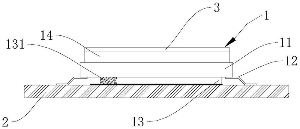
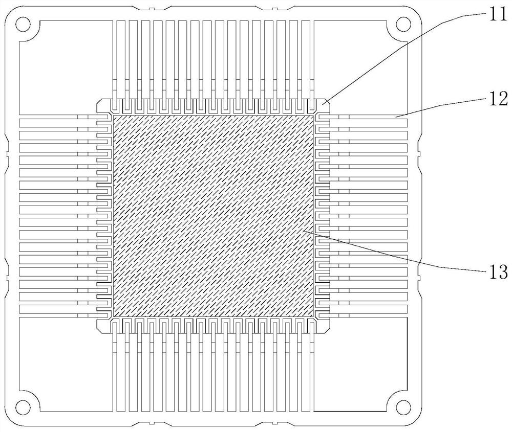
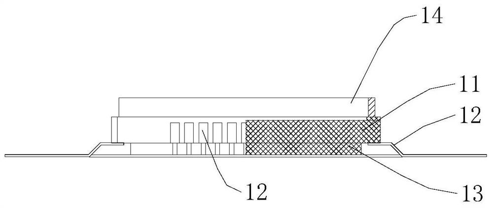
[0024] see Figure 1 to Figure 7 The ceramic four-sided flat package housing 1 includes a ceramic housing 11 and a plurality of leads 12. The ceramic housing 11 is used to carry a chip. The lead wires 12 are drawn from the bottom of the ceramic housing 11 to the surroundings. For the boss 13 extending downward, the height difference between the bottom plane of the boss 13 and the lowest point of the lead wire 12 is 0-0.15 mm.

[0025] Compared with the prior art, the bottom of the ceramic housing 11 in the ceramic quadrilateral flat package housing 1 of the presen...


PUM


Abstract

The invention provides a ceramic four-side flat packaging shell and a ceramic four-side flat packaging device. The ceramic four-side flat packaging shell comprises a ceramic shell body and a plurality of leads, the ceramic shell body is used for bearing a chip, the leads are led out from the bottom of the ceramic shell body to the periphery, the bottom of the ceramic shell body is further provided with a boss extending downwards, and the height difference between the bottom plane of the boss and the lowest point of each lead is 0-0.15 mm. The height difference between the bottom plane of the boss and the lowest point of the lead is 0-0.15 mm, and the gap between an existing packaging shell and a PCB is about 0.50-1.0 mm, so that the gap between the ceramic four-side flat packaging shell and the PCB is reduced, the thickness of an adhesive layer for reinforcement is reduced, the board-level reinforcement is reliable, the stress of the lead can be effectively reduced, the lead is prevented from being deformed or damaged, and high reliability of a mounted device is ensured.

Description

technical field [0001] The invention belongs to the technical field of packaging of microelectronic integrated circuits, and more specifically relates to a ceramic quadrilateral flat package shell and a ceramic quadrilateral flat package device. Background technique [0002] Ceramic quad flat package (CQFP, ceramic quad flat package) is a surface mount component packaging type, due to its small size, small parasitic parameters, mature manufacturing technology, excellent electrical performance and heat dissipation performance, and high reliability, etc. The reason is that it is widely used in core devices such as field programmable gate array FPGA and digital signal processor DSP, and has been widely used in high reliability fields such as military, aviation, aerospace, medical electronics, and large-scale computers. [0003] When connecting the CQFP device to the PCB board, since there is a height difference of 0.5 to 1 mm between the bottom of the ceramic quad flat package ...

Claims


Application Information

Patent Timeline
Patent Type & Authority Applications(China)
IPC IPC(8): H01L23/04H01L23/053
CPCH01L23/04H01L23/053
Inventor 杨振涛彭博高岭于斐刘林杰毕大鹏淦作腾王东生张腾刘彤
Owner THE 13TH RES INST OF CHINA ELECTRONICS TECH GRP CORP
Why Eureka
Try Eureka