Double-resistance photoelectric protection film preparation method and double-resistance photoelectric protection film
A protective film, photoelectric technology
- Summary
- Abstract
- Description
- Claims
- Application Information
AI Technical Summary
Problems solved by technology
Method used
Image
Examples
Embodiment Construction
[0029] The specific embodiment of the present invention will be described in further detail by describing the embodiments below with reference to the accompanying drawings, the purpose is to help those skilled in the art to have a more complete, accurate and in-depth understanding of the concept and technical solutions of the present invention, and contribute to its implementation.
[0030] The invention provides a method for preparing a double anti-photoelectric protective film, comprising the following steps:
[0031] S1, unwinding;
[0032] S2, gluing;
[0033] S3, drying;
[0034] S4, winding.
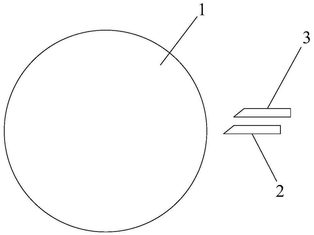
[0035] Specifically, in the above step S1, the base film is unrolled by the unwinding drum, and the unrolled base film is transported to the coating machine by the guide roller. In the above step S2, the rotating glue roller 1 applies the glue solution to the surface of the base film. In the above step S3, the protective film coated with glue is transported to a drying box by ...
PUM
| Property | Measurement | Unit |
|---|---|---|
| thickness | aaaaa | aaaaa |
| thickness | aaaaa | aaaaa |
Abstract
Description
Claims
Application Information


