

Semiconductor process execution method
A technology for semiconductors and process recipes, applied in machine execution devices, address formation of the next instruction, instruments, etc., can solve problems such as fixed data structure, low recipe execution efficiency, and limited product expansion space.
- Summary
- Abstract
- Description
- Claims
- Application Information
AI Technical Summary
Problems solved by technology
Method used
Image

Examples
Embodiment Construction
[0051] Specific embodiments of the present invention will be described in detail below in conjunction with the accompanying drawings. It should be understood that the specific embodiments described here are only used to illustrate and explain the present invention, and are not intended to limit the present invention.
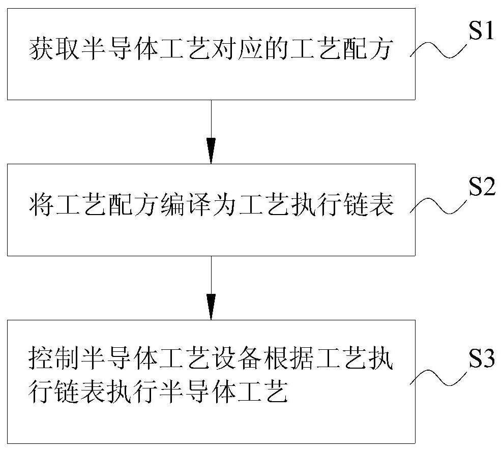
[0052] As an aspect of the present invention, a method for executing a semiconductor process is provided, such as figure 1 As shown, the method includes:
[0053] In step S1, the process recipe corresponding to the semiconductor process is obtained. The process recipe is in plain text format, including hardware instructions and process flow instructions. The hardware instructions and process flow instructions are both strings. The hardware instructions are used to control the semiconductor process equipment to execute the semiconductor process. process steps, the process flow instructions are used to control the process flow of the semiconductor process;
[00...
PUM
 Abstract
Description
Claims
Application Information