
Semiconductor light-emitting element

A light-emitting element and semiconductor technology, which is applied in semiconductor devices, electrical components, circuits, etc., can solve the problems of aging light attenuation, many defects, and poor quality

Active Publication Date: 2021-09-14
XIAMEN SILAN ADVANCED COMPOUND SEMICON CO LTD +1
View PDF5 Cites 1 Cited by
  • Summary
  • Abstract
  • Description
  • Claims
  • Application Information

AI Technical Summary

Problems solved by technology

[0003] The well layer and the barrier layer of the quantum well layer of the existing ultraviolet semiconductor light-emitting element have many defects, and the quality is poor, which easily causes aging light attenuation; at the same time, the Si in the quantum well layer and the Mg in the p-type semiconductor layer If the distance is too close, it is easy to cause Mg and Si to mix due to element migration and diffusion under high temperature or long-term use, which will cause aging light attenuation phenomenon, making the aging light attenuation of 1000 hours generally more than 30%, or even more than 50%.

Method used


Image

  • Semiconductor light-emitting element

Examples


Embodiment Construction

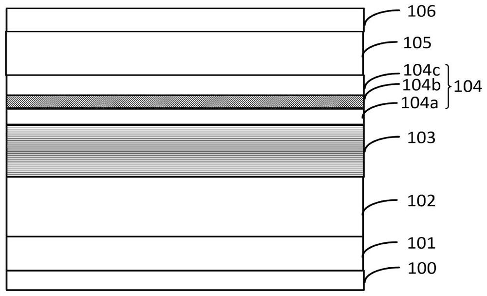
[0025] The well layer and the barrier layer of the quantum well layer of the existing ultraviolet semiconductor light-emitting element have many defects, and the quality is poor, which easily causes aging and light decay; meanwhile, Si and p-type semiconductor layers (such as Al in the quantum well layer) y Ga 1-y The distance of Mg in the N layer) is too close, it is easy to cause Mg and Si to mix under the condition of high temperature or long-term use due to element migration and diffusion, thereby causing aging light attenuation phenomenon, so that the aging light attenuation of 1000 hours is generally above 30%. Even above 50%.

[0026] In order to improve the aging luminescence attenuation performance of semiconductor light-emitting elements, especially ultraviolet semiconductor light-emitting elements, the present invention provides a semiconductor light-emitting element, adding non-doped aging light attenuation control between the doped quantum well layer and the P-typ...


PUM

PropertyMeasurementUnit
Thicknessaaaaaaaaaa
Thicknessaaaaaaaaaa
Thicknessaaaaaaaaaa

Abstract

The invention provides a semiconductor light-emitting element, which sequentially comprises a substrate, an n-type semiconductor layer, a doped quantum well layer, an aging light attenuation control layer and a p-type semiconductor layer from bottom to top, the aging light attenuation control layer sequentially comprises a non-doped quantum well layer, a first light attenuation control layer and / or a second light attenuation control layer from bottom to top, wherein the non-doped quantum well layer is provided with at least one non-doped barrier layer. The aging light attenuation control layer is added between the doped quantum well layer and the p-type semiconductor layer, so that the probability that Si of the doped quantum well layer is in diffusion contact with Mg of the p-type semiconductor layer in the long-term aging process can be reduced, the aging light attenuation performance of the semiconductor light-emitting element, especially an ultraviolet semiconductor light-emitting element, is improved, and the light decay after aging for 1000 hours is reduced from 30% or more (even 50% or more) to 10% or less.

Description

technical field [0001] The invention relates to the technical field of semiconductors, in particular to a semiconductor light emitting element. Background technique [0002] Ultraviolet semiconductor light-emitting element, with a wavelength range of 200-300nm, the ultraviolet light emitted can interrupt the DNA or RNA of viruses and bacteria, directly kill viruses and bacteria, and can be widely used in air purification, tap water sterilization, household air conditioning sterilization, automobile Sterilization and disinfection fields such as air-conditioning sterilization. [0003] The well layer and the barrier layer of the quantum well layer of the existing ultraviolet semiconductor light-emitting element have many defects, and the quality is poor, which easily causes aging light attenuation; at the same time, the Si in the quantum well layer and the Mg in the p-type semiconductor layer If the distance is too close, it is easy to cause Mg and Si to mix due to element mi...

Claims


Application Information

Patent Timeline
IPC IPC(8): H01L33/06H01L33/12H01L33/14H01L33/32H01L33/00
CPCH01L33/06H01L33/12H01L33/145H01L33/325H01L33/0075A61L9/20C02F1/325C02F2303/04H01L33/025
Inventor 郑锦坚高默然毕京锋范伟宏曾家明张成军
Owner XIAMEN SILAN ADVANCED COMPOUND SEMICON CO LTD
Learn More