

Semiconductor device
A semiconductor and device technology, applied in the structural field of high-voltage semiconductor devices, can solve problems such as transistor performance degradation, achieve the effect of reducing channel resistance and improving performance
- Summary
- Abstract
- Description
- Claims
- Application Information
AI Technical Summary
Problems solved by technology
Method used
Image

Examples
Embodiment 1
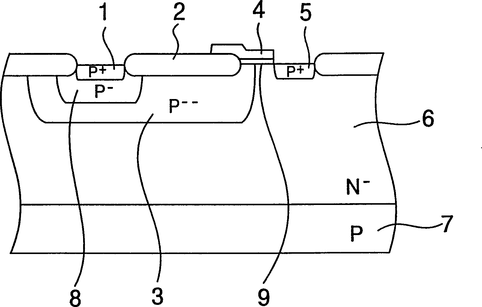
[0023] figure 1 It is a semiconductor device, mainly composed of the following parts: P + Type drain diffusion layer 1, local Si oxide layer 2, low concentration P -- Type electric field relaxation layer 3, polysilicon gate 4, P + Type source diffusion layer 5, N - Type well diffusion layer 6, P type semiconductor substrate 7, formed in low concentration P -- Moderate concentration of P in type electric field relaxation layer 3 - Type diffusion layer 8, gate oxide film 9. where low concentrations of P -- The role of the type electric field relaxation layer 3 in the semiconductor device of the present invention is the same as that in the traditional transistor: that is, the load on the P + type drain diffusion layer 1 and P + type source diffusion layer 5 voltage between the N - Type well diffused layer 6 and P -- The depletion layer extending between the type electric field relaxation layers 3 bears. The present invention is characterized in that it provides a mediu...
Embodiment 2
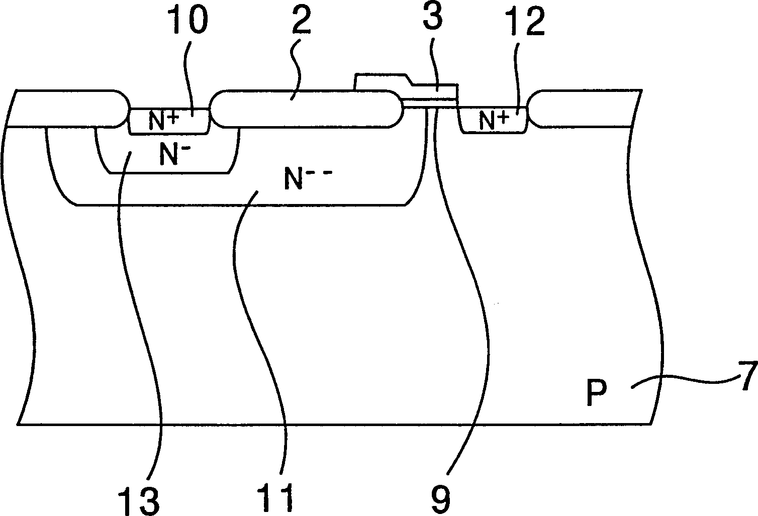
[0027] figure 2 It is a semiconductor device, mainly composed of the following parts: N + Type drain diffusion layer 10, local Si oxide layer 2, low concentration N -- Type electric field relaxation layer 11, gate 3, N + Type source diffusion layer 12, P type semiconductor substrate 7, formed in low concentration N -- Moderate concentration N in type electric field relaxation layer 11 - Type diffusion layer 13, gate oxide film 9. where low concentration of N -- The role of the type electric field relaxation layer 11 in the semiconductor device of the present invention is the same as that in the traditional transistor: that is, it is loaded on the N + type drain diffusion layer 10 and N + type source diffusion layer 12 by a voltage between P - type semiconductor substrate 7 and N -- The depletion layer extending between the type electric field relaxation layers 11 bears. The present invention is characterized in that it provides a medium concentration N - Type diffus...
Embodiment 3
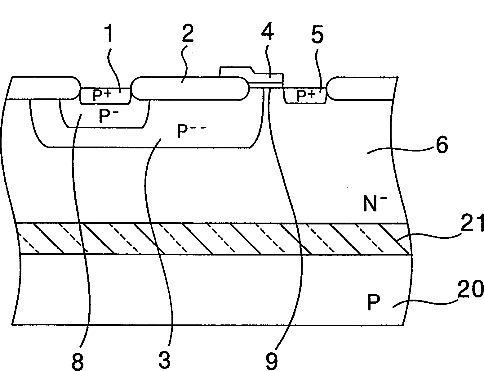
[0031] image 3 It is a semiconductor device, mainly composed of the following parts: P + Type drain diffusion layer 1, local Si oxide layer 2, low concentration P -- Type electric field relaxation layer 3, gate 4, P + Type source diffusion layer 5, N - Type fully diffused layer 6, oxide buried layer 21, P - Type support substrate 20, formed in low concentration P -- Moderate concentration of P in type electric field relaxation layer 3 - Type diffusion layer 8, gate oxide film 9.
[0032] where low concentrations of P -- The function of the type electric field relaxation layer 3 in the semiconductor device of the present invention is the same as that in a conventional transistor. In embodiment 3, a layer of oxide buried layer 21 is covered on the P-type support substrate, and become an insulating isolation substrate, which serves as a P-type semiconductor substrate, instead of figure 1 The P-type semiconductor substrate in Embodiment 1 is shown, and its operation is t...
PUM
 Abstract
Description
Claims
Application Information