Connector manufacturing method, electronic equipment, connector and application

A manufacturing method and connector technology, applied in the direction of electrical connection of printed components, structural connection of printed circuits, printed circuits, etc., can solve the problems of large connection area, low cost, high parasitic parameters, etc., and achieve stable transmission of high-speed signals , the effect of small footprint and large number of pins

Pending Publication Date: 2021-09-24
FOCALCREST LTD
View PDF7 Cites 0 Cited by
  • Summary
  • Abstract
  • Description
  • Claims
  • Application Information

AI Technical Summary

Problems solved by technology

[0003] Connectors are generally single-row or double-row, and can only be made into straight strips, which have an impact on PCB design space and component layout, and the cost is high
Another connection method is to connect two PCB boards with a half-hole on the side of the board. This method is low in cost, but only places components on one side. The overall connection area is large and the parasitic parameters are high, which affects the performance of high-speed signals on the PCB.

Method used


Image

  • Connector manufacturing method, electronic equipment, connector and application
  • Connector manufacturing method, electronic equipment, connector and application
  • Connector manufacturing method, electronic equipment, connector and application

Examples


Embodiment Construction

[0029] The following will clearly and completely describe the technical solutions in the embodiments of the present invention with reference to the accompanying drawings in the embodiments of the present invention. Obviously, the described embodiments are only some, not all, embodiments of the present invention. Based on the embodiments of the present invention, all other embodiments obtained by those skilled in the art without creative efforts fall within the protection scope of the present invention.

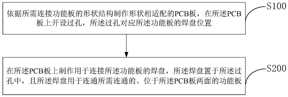
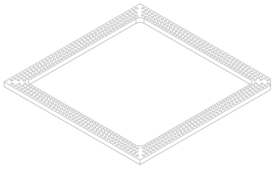
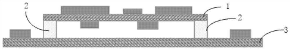
[0030] see figure 1 , figure 1 It is a structural schematic diagram of an embodiment of a method for manufacturing a connector in an embodiment of the present invention. can be combined Figure 6 and Figure 7 Understand; Described connector making method comprises the following steps:

[0031] Step S100: Make a PCB board with a matching shape according to the shape and structure of the functional board to be connected, and open a via hole on the PCB board, and the via hol...


PUM


Abstract

The invention discloses a connector manufacturing method, electronic equipment, a connector and application. The method comprises the steps that a PCB matched with a function board in shape is manufactured according to the shape and structure of the function board needing to be connected, a via hole is formed in the PCB, and the via hole corresponds to the position of a bonding pad of the function board; bonding pads used for being connected with the function boards are manufactured on the PCB, the bonding pads are arranged in the via holes, and the bonding pads are used for being communicated with the function boards which need to be communicated and are located on the two faces of the PCB. In the technical scheme provided by the invention, the connector using the PCB as the carrier can be made into any shape, the number of pins is large, the occupied area is small, high-speed stable signal transmission can be realized through the design of the bonding pad and the distance, the PCB does not need to place elements on a single surface, and the cost is lower than that of a common connector.

Description

technical field [0001] The invention relates to the field of connectors, in particular to a connector manufacturing method, electronic equipment, connectors and applications. Background technique [0002] At present, the board-to-board connector between PCBs is supported by plastic, and metal strips or metal sheets are used as pins to connect the PCBs. [0003] Connectors are generally single-row or double-row, and can only be made into straight lines, which will affect the PCB design space and component layout, and the cost is high. Another connection method is to connect two PCB boards with half-holes on the side of the board. This method is low in cost, but only places components on one side. The overall connection area is large and the parasitic parameters are high, which affects the performance of high-speed signals on the PCB. [0004] Therefore prior art still needs further development. Contents of the invention [0005] In view of the above technical problems, th...

Claims


Application Information

Patent Timeline
IPC IPC(8): H05K3/00H05K3/30H05K1/14H05K1/11
CPCH05K3/0044H05K3/303H05K1/14H05K1/111H05K1/144H05K1/113H05K3/3436H05K3/368H05K2201/042H05K2201/10378H05K2201/09481H05K2201/09563Y02P70/50G06F30/392H05K3/4007H05K2201/0367H05K3/40
Inventor 谢文杰刘振宇谭伟圣
Owner FOCALCREST LTD
Why Eureka
Try Eureka