Method for manufacturing an embedded package and structure thereof

Inactive Publication Date: 2015-01-15
APTOS TECH
View PDF5 Cites 6 Cited by
  • Summary
  • Abstract
  • Description
  • Claims
  • Application Information

AI Technical Summary

Benefits of technology

[0007]The primary object of the present invention is to provide a package m

Problems solved by technology

But design of SoC takes a great deal of time, and packaging different elements on one IC still takes significant area on the produced IC, hence its range of application is limited.
However, through silicon via (TSV) technique has a much higher technical threshold and manufacturing cost, thus it is not widely adopted yet.
However, the ICs befor

Method used


Image

  • Method for manufacturing an embedded package and structure thereof
  • Method for manufacturing an embedded package and structure thereof
  • Method for manufacturing an embedded package and structure thereof

Examples


first embodiment

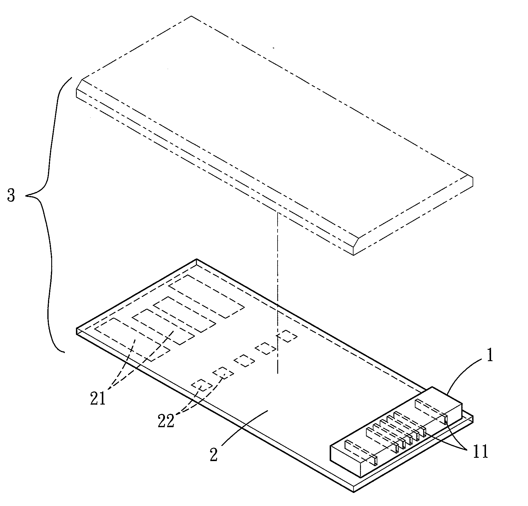
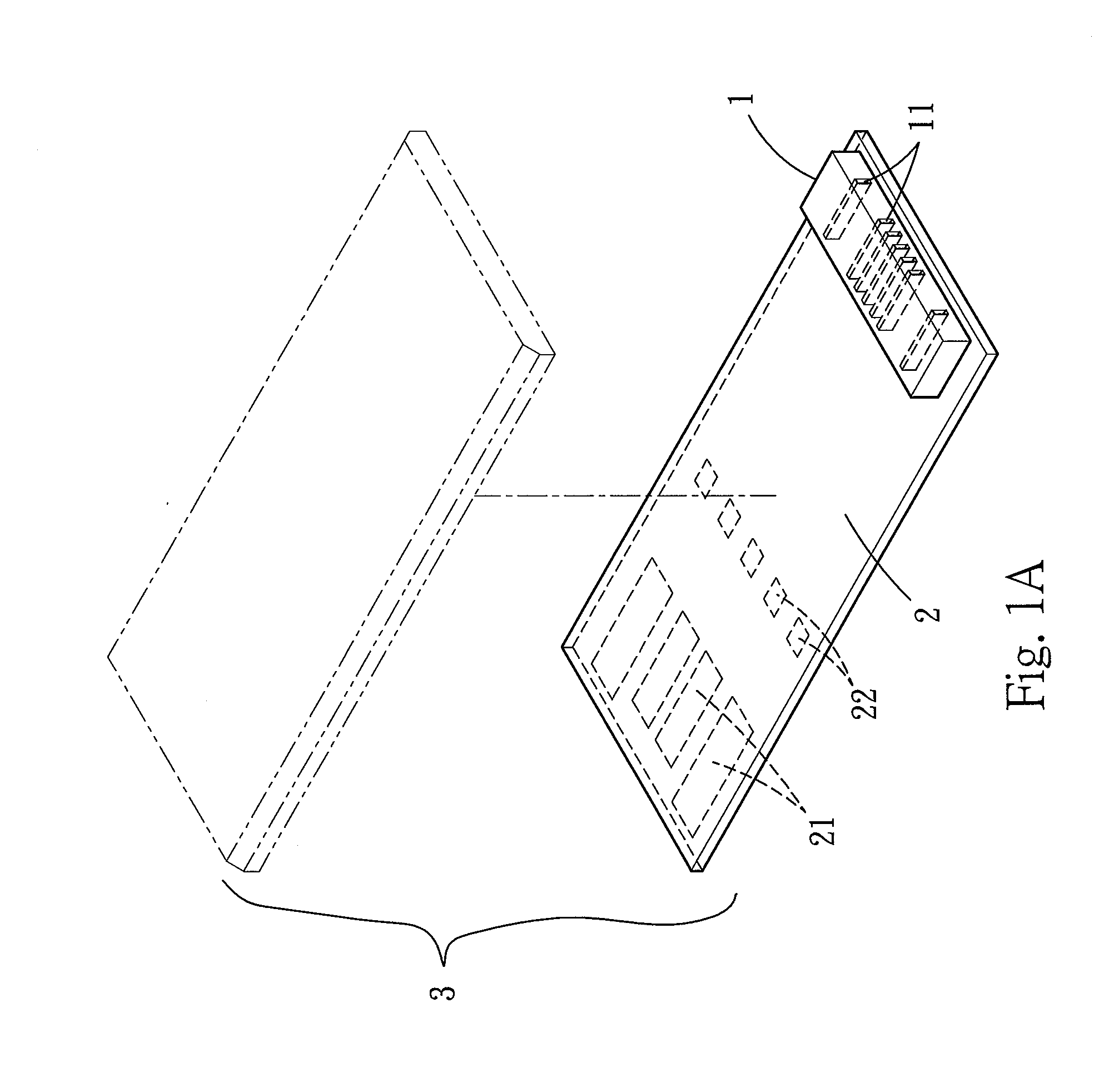
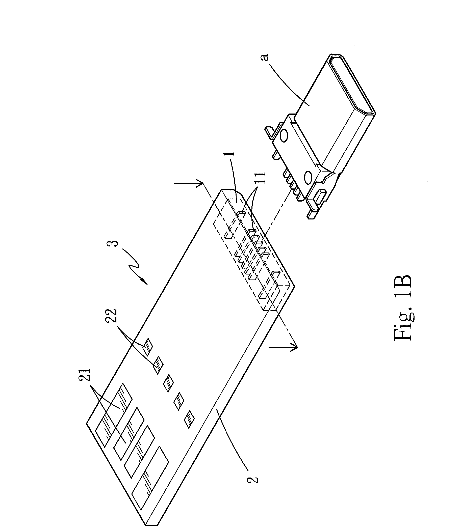
[0033]Please refer to FIGS. 1A through 6 for the method for manufacturing an embedded package according to the invention. To facilitate discussion, a manufacturing process of a USB 3.0 / Micro-USB dual connector flash drive is used as an example below. The manufacturing process comprises:

[0034]Step 1: Referring to FIG. 1A, coupling an first embedded body 1 including a plurality of connection ports 11 with a first circuit substrate 2 which has flash memory chips (not shown in the drawings), a control circuit (also not shown in the drawings) and metal contacts 21 and 22 for USB 2.0 and USB 3.0. The first embedded body 1 can be male or female formed by an epoxy molding compound (EMC) or through injection molding. A female seat is employed as an embodiment for discussion below. After the first embedded body 1 (or the first embedded body 1a shown in FIG. 2) is coupled with the first circuit substrate 2, they are packaged into a package 3, and the connection ports 11 are not yet exposed at ...

second embodiment

[0039]At present the general multi-chip package (MCP) technology integrates and packages two or more memory chips in a same Ball Grid Array (BGA) package through horizontal positioning and / or vertical stacking manner. the invention also provides a novel application for the MCP technology. Please referring to FIGS. 7 through 9, the method includes:

[0040]Step 1: coupling a plurality of first embedded bodies 1b each includes a plurality of connection ports 11b with a first circuit substrate 2b including multiple chips c or electronic elements d, and packaging them to form a package 3b which can be a BGA or Land Grid Array (LGA) with high pin count. In this embodiment a BGA package 3b is used. The first circuit substrate 2b has pins extended to each side thereof so that the first embedded bodies 1b can be positioned at four sides of the first circuit substrate 2b.

[0041]Step 2: cutting the four sides of the package 3b to expose the connection ports 11b and make them open at four sides o...

embodiment 2

[0050]Similarly, as shown in FIG. 14, to produce the MCP or SiP as mentioned in the embodiment 2, a plurality of first embedded bodies 1h including multiple connection ports (not shown in the drawing) can be arranged in a preset layout on a first circuit substrate or a substrate 9 made of a wafer and packaged. Then the substrate 9 is cut according to preset paths corresponding to the arranged layout (indicated by solid lines in the drawing) to form multiple independent package elements and expose the connection ports.

[0051]The method of positioning the first embedded bodies and performing cutting after packaging them (not limited to the drawings or description depicted above) as discussed above can further reduce manufacturing time and improve production efficiency.

[0052]It is to be noted that the first circuit substrates 2, 2b, 2d, 2e and 2f discussed in the previous embodiments can also be implemented like a package loading board with a separable metal layer disclosed in R.O.C. pa...


PUM

PropertyMeasurementUnit
Timeaaaaaaaaaa
Electrical conductoraaaaaaaaaa

Abstract

A method for manufacturing an embedded package comprises the steps of: coupling at least one first embedded body including at least one connection port with a first circuit substrate and packaging the first embedded body and the first circuit substrate to form a package; and exposing the connection port of the package on an outer side of the package for other electronic carriers to couple with. The invention can overcome the disadvantage of the conventional System in Package manufacturing process which integrally packages multiple ICs in a same package to result in discard of the entire package because of failure of a single IC. The method of the invention makes assembly simpler, expansion, test and replacement of IC components easier, and also can reduce manufacturing time and accumulated heat, lower the cost and improve yield rate.

Description

FIELD OF THE INVENTION[0001]The present invention relates to a method for manufacturing a package and structure thereof, particularly an integrated package comprising an embedded body and the structure thereof.BACKGROUND OF THE INVENTION[0002]In recent years semiconductor package technology includes two-dimensional System on Chip (SoC) which aims to cluster electronic systems into integrated circuits formed on a single chip. It has many advantages such as lower power consumption, higher performance and smaller package area. But design of SoC takes a great deal of time, and packaging different elements on one IC still takes significant area on the produced IC, hence its range of application is limited.[0003]System in Package (SiP) is a newly developed package technique which deploys all or most electronic functions of a system or sub-system in an integrated substrate. Compared with SoC it has many benefits such as smaller size, higher performance, shorter development cycle and lower ...

Claims


Application Information

Patent Timeline
IPC IPC(8): H05K1/18H05K3/30H05K1/11
CPCH05K1/111H05K1/188Y10T29/49146Y10T29/4913H05K3/303H01L2924/0002H01R12/724H05K1/185H05K2201/10189H01L2924/00
Inventor LUNG, CHEN HSUANLU, CHIEN HSIENCHENG, YA YUNLIN, KUO HUA
Owner APTOS TECH
Why Eureka
Try Eureka