Flexible leaded stacked semiconductor package

Inactive Publication Date: 2006-05-04
TEXAS INSTR INC
View PDF10 Cites 24 Cited by
  • Summary
  • Abstract
  • Description
  • Claims
  • Application Information

AI Technical Summary

Benefits of technology

[0015] The vertical alignment of first and second assemblies is preferably achieved during the loading process of the mold cavity, especially for devices having the first assembly using a leadframe of the leadless category. After the

Problems solved by technology

In some proposals, though, the chips are stacked, but usually interconnected by techniques, which turn out to be not cost-effective in fabrication (beam lead technology, tape automated bonding, multi-level substrates, etc.).

Method used


Image

  • Flexible leaded stacked semiconductor package
  • Flexible leaded stacked semiconductor package
  • Flexible leaded stacked semiconductor package

Examples


Example

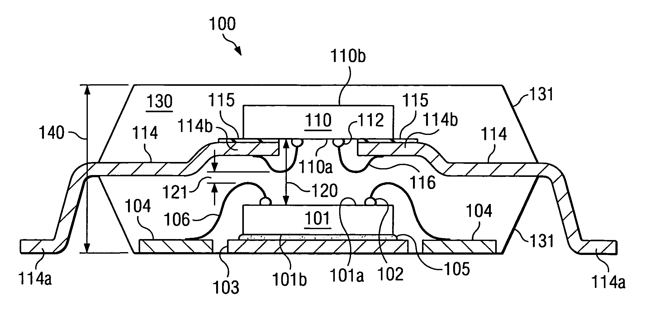
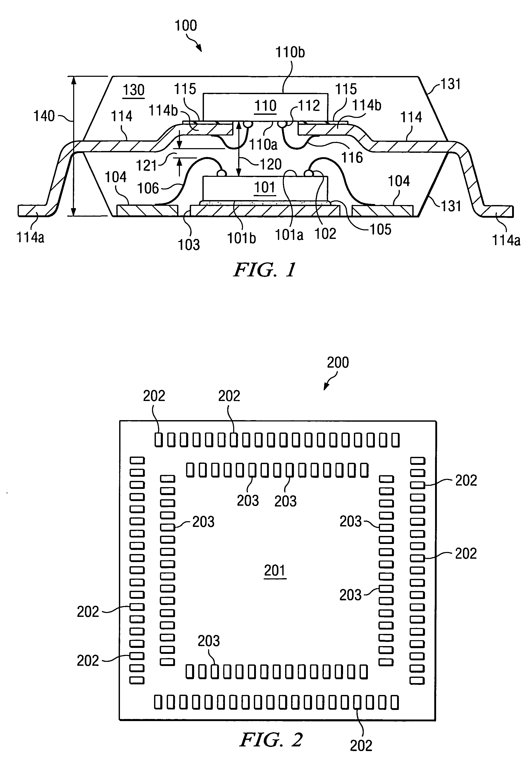
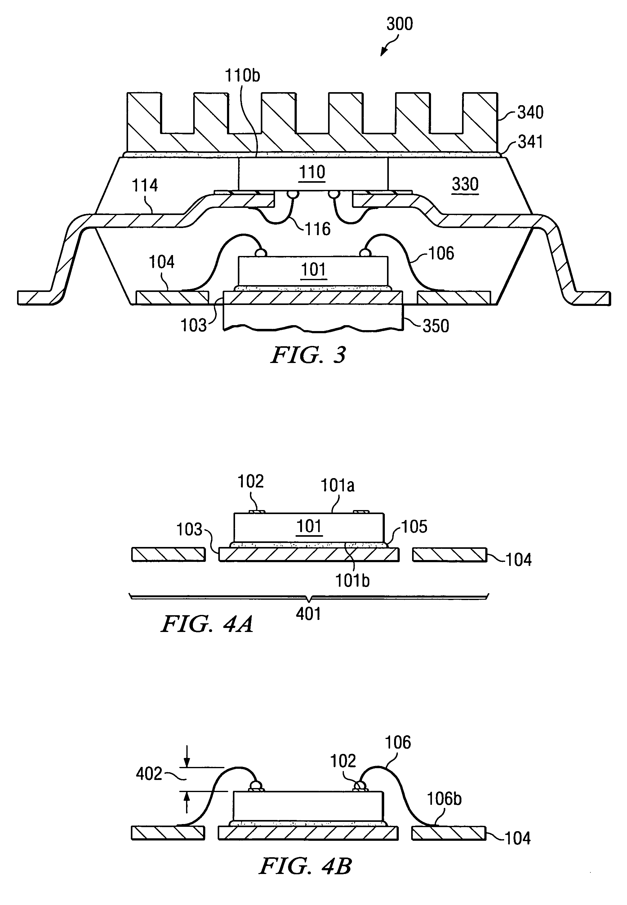
[0026]FIG. 1 displays an embodiment of the invention; the schematic cross section shows a stacked multichip semiconductor device, generally designated 100, comprising two semiconductor assemblies. The first assembly comprises a first chip 101, which has an active surface 101a including an integrated circuit and / or operating discrete components, and a plurality of bond pads 102; chip 101 also has a passive surface 101b. The first semiconductor assembly further has a first leadframe consisting of a chip mount pad 103 and a plurality of leads 104. In the example of FIG. 1, leads 104 are configured as metal pieces shaped for a leadframe designed for a so-called “leadless device”. Leads 104 provide the input / output terminals for the first semiconductor assembly and may be attached to external parts (for example, by pressure contact or by soldering).

[0027] For many devices, chip 101 is made of silicon; other alternatives include silicon germanium, gallium arsenide or other semiconductor ...


PUM


Abstract

A multi-chip semiconductor device comprises two semiconductor assemblies vertically aligned so that the second active chip surface (110a) faces the first active chip surface (101a) and forms a gap (120) between the assemblies. Encapsulation material (130) fills the gap and couples the first and second assemblies together to form the multi-chip device (100). Lead portions of the first and second leadframes remain exposed from the encapsulation material. The exposed leads (104) of the first leadframe may be comprised for leadless assembly, and the exposed leads (114a) of the second leadframe may be formed coplanar with the first leads (104).

Description

FIELD OF THE INVENTION [0001] The present invention is related in general to the field of semiconductor devices and processes, and more specifically to assembly methods for integrated circuit chips resulting in stacked multichip devices in a single package. DESCRIPTION OF THE RELATED ART [0002] It is advantageous for many applications of semiconductor devices to arrange the needed devices in close proximity. When only two, or few more, semiconductor chips are needed, various arrangements have been proposed in order to achieve the desired proximity, and to enable a minimization of required space. Typically, these arrangements are planar assemblies of semiconductor chips on a substrate, with or without a specific encapsulation. For these arrangements, the term “multichip module” is commonly used. For an encapsulated assembly, the term “multichip package” has been introduced. For many years, there has been a rather limited market for multichip modules and multichip packages, but driven...

Claims


Application Information

Patent Timeline
IPC IPC(8): H01L21/48H01L23/495
CPCH01L21/565H01L23/4951H01L23/49537H01L23/49575H01L2224/48091H01L2224/48247H01L2224/4826H01L2224/48465H01L2224/73215H01L2224/73265H01L2224/92H01L2224/92247H01L2924/01013H01L2924/01029H01L2924/01046H01L2924/01079H01L2924/00014H01L24/48H01L2224/32245H01L2224/92147H01L2924/00H01L2924/00012H01L2924/15747H01L2924/14H01L2224/45124H01L2224/45147H01L2224/45144H01L24/45H01L2224/45014H01L2924/181H01L2224/45015H01L2924/207H01L2924/206
Inventor MATSUNAMI, AKIRA
Owner TEXAS INSTR INC
Why Eureka
Try Eureka