Semiconductor device

A semiconductor and conductive technology, applied in the direction of semiconductor devices, transistors, electric solid-state devices, etc., can solve the problems of reduced diode damage tolerance, increased recovery current, etc.

Pending Publication Date: 2021-09-28
MITSUBISHI ELECTRIC CORP
View PDF1 Cites 0 Cited by
  • Summary
  • Abstract
  • Description
  • Claims
  • Application Information

AI Technical Summary

Problems solved by technology

[0005] However, in the semiconductor device in which the insulated gate bipolar transistor and the diode are formed on one semiconductor substrate as described above, since holes, which are minority carriers, flow from the insulated gate bipolar transistor region to the diode region, the Compared with the case where an insulated gate bipolar transistor and a diode are connected in parallel as a separate component, there is a problem that the recovery current during the recovery operation becomes larger and the breakdown resistance of the diode decreases.

Method used


Image

  • Semiconductor device
  • Semiconductor device
  • Semiconductor device

Examples


Embodiment approach 1

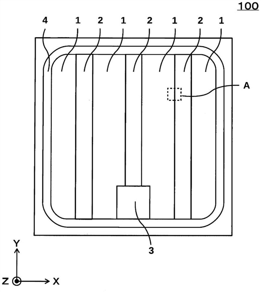
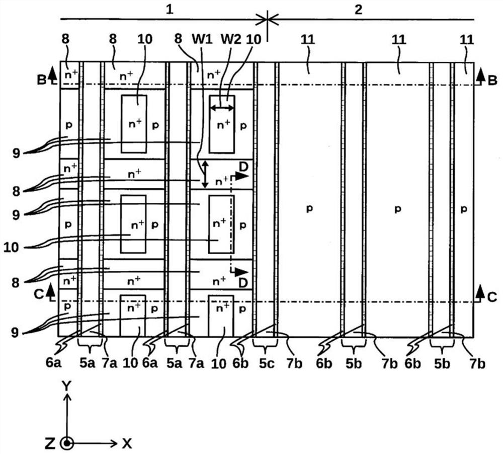
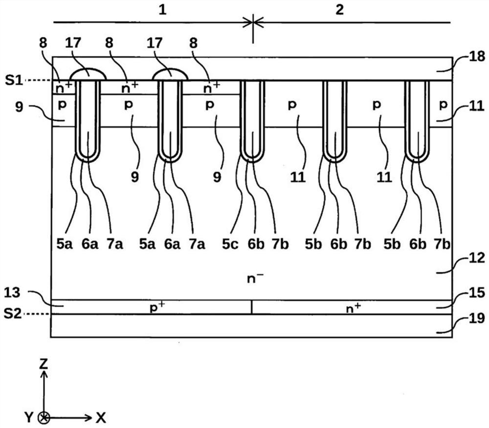
[0030] use Figure 1 to 5 The structure of the semiconductor device according to the first embodiment will be described. figure 1 and figure 2 It is a top plan view showing the semiconductor device according to the first embodiment. figure 2 Be figure 1 The top view of the amplified A portion is amplified, and is a top plan view showing the structure of the first main surface side of the semiconductor substrate. exist figure 2 The electrodes such as electrodes provided on the upper side of the first main surface of the semiconductor substrate are omitted. Figure 3 to 5 It is a cross-sectional view showing the semiconductor device according to the first embodiment. image 3 Yes figure 2 A cross-sectional view of the B-B line recorded. Figure 4 Yes figure 2 A cross-sectional view of the C-C line recorded. Figure 5 Yes figure 2 A cross-sectional view of the D-D line recorded. exist Figure 1 to 5 In order to facilitate explanation, the XYZ orthogonal coordinate axis representing the dir...

Embodiment approach 2

[0083] use Figure 13 and Figure 14 The structure of the semiconductor device according to the second embodiment will be described. Figure 13 and Figure 14 It is a plan view showing the semiconductor device according to the second embodiment. Figure 14 Be Figure 13 The diagram recorded in the e-part is an enlarged plan view showing the structure of the first main surface side of the semiconductor substrate. exist Figure 14 The electrodes such as electrodes provided on the upper side of the first main surface of the semiconductor substrate are omitted. exist Figure 13 and Figure 14 In order to facilitate explanation, the XYZ orthogonal coordinate axis representing the direction is also shown. Further, in Embodiment 2, the same components as those in the first embodiment, the same structure elements are identical, and the description thereof will be omitted.

[0084] like Figure 13 As shown, in the semiconductor device 200 according to the second embodiment, the insulating gate type ...

Embodiment approach 3

[0092] use Figure 15 and Figure 16 The structure of the semiconductor device according to the third embodiment will be described. Figure 15 and Figure 16 It is a plan view showing the semiconductor device according to the third embodiment. Figure 16 Be Figure 15 The diagram recorded in the F portion is enlarged, and is a plan view showing the configuration of the first main surface side of the semiconductor substrate. exist Figure 16 The electrodes such as electrodes provided on the upper side of the first main surface of the semiconductor substrate are omitted. exist Figure 15 and Figure 16 In order to facilitate explanation, the XYZ orthogonal coordinate axis representing the direction is also shown. Further, in Embodiment 3, the same structural elements as those described in Embodiments 1 and 2 are identical, and the same reference numerals are labeled and the description thereof will be omitted.

[0093] like Figure 15 As shown, in the semiconductor device 300 according to the...


PUM


Abstract

The invention provides a semiconductor device which can enhance the breakdown resistance during the recovery operation. The semiconductor device (100) includes an insulated gate bipolar transistor region (1) and a diode region (2) adjacent to each other, wherein the insulated gate bipolar transistor region (1) includes base layers (9) of a second conductive type provided on the first main surface side, emitter layers (8) of the first conductive type selectively provided in a surface layer of the base layer (9) on the first main surface side, multiple gate electrodes (7a) provided on the first main surface side of the semiconductor substrate, aligned in a first direction extending along the first main surface, and facing the emitter layer (8), the base layer (9), and the drift layer (12) via a gate insulating film (6a), carrier injection suppression layers (10) of the first conductive type selectively provided in a surface layer of the base layer (9) on the first main surface side and sandwiched by the base layers (9) in the first direction.

Description

Technical field [0001] The present invention relates to a semiconductor device. Background technique [0002] From the perspective of energy conservation, the inverter device is widely used in the field of home appliances, electric vehicles, railways. Most of the inverter device is made of an insulating gate type bipolar transistor (IGBT: Insuated Gate Bipolar Transistor) and the continuous flow diode. The insulating gate type bipolar transistor and diode are connected in the inside of the inverter device through a wire or the like. [0003] In order to the inverter device miniaturization, a semiconductor device (e.g., Patent Document 1) is proposed in a semiconductor substrate. [0004] Patent Document 1: Japanese Laid-Open 2008-103590 [0005] However, in the above-mentioned semiconductor substrate, a semiconductor device having an insulated gate type bipolar transistor and a diode is formed, since a small number of carriers, the hole is flowed into the diode region from the in...

Claims


Application Information

Patent Timeline
Patent Type & Authority Applications(China)
IPC IPC(8): H01L29/06H01L29/739H01L27/06
CPCH01L27/0629H01L29/0684H01L29/7398H01L29/7397H01L29/0615H01L29/8613H01L29/407H01L27/0727H01L29/0696H01L29/0834H01L29/66348H01L29/063H01L29/1095H01L29/7804H01L29/7302
Inventor 中谷贵洋新田哲也大塚翔瑠
Owner MITSUBISHI ELECTRIC CORP
Why Eureka
Try Eureka