Semiconductor device and method for manufacturing same

A semiconductor, opposite-side technology, used in semiconductor/solid-state device manufacturing, semiconductor devices, semiconductor/solid-state device components, etc.

Active Publication Date: 2017-08-01
DENSO CORP
View PDF7 Cites 3 Cited by
  • Summary
  • Abstract
  • Description
  • Claims
  • Application Information

AI Technical Summary

Problems solved by technology

Therefore, during reflow, there is a possibility that the second solder may infiltrate and expand on the surface of the metal component and flow into the s

Method used


Image

  • Semiconductor device and method for manufacturing same
  • Semiconductor device and method for manufacturing same
  • Semiconductor device and method for manufacturing same

Examples


no. 1 Embodiment approach

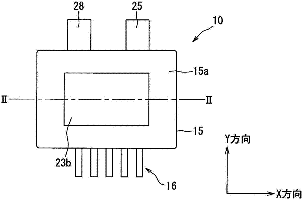
[0049] First, based on Figure 1 ~ Figure 3 , the schematic structure of the semiconductor device will be described.

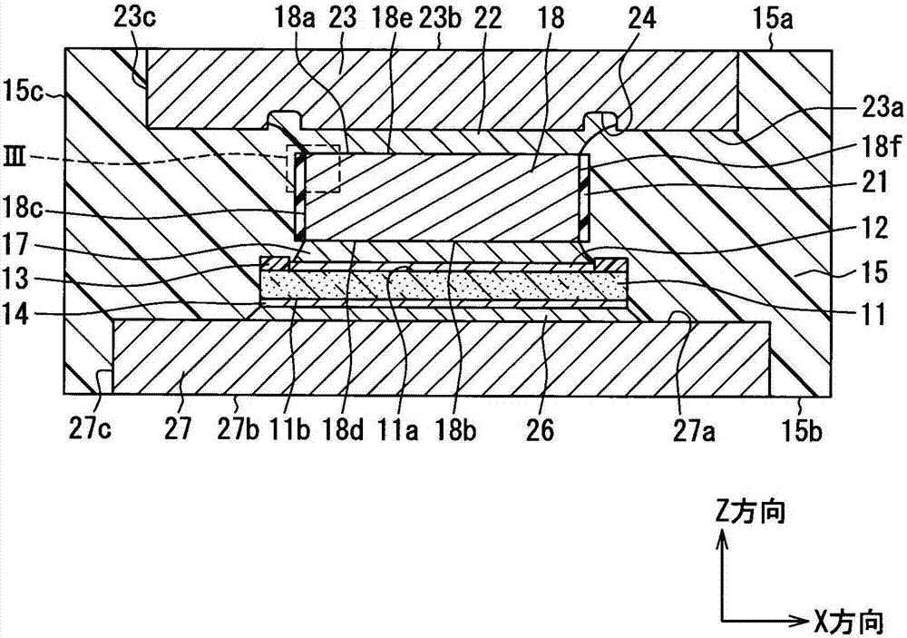
[0050] Such as figure 1 as well as figure 2 As shown, the semiconductor device 10 includes a semiconductor chip 11 , a sealing resin body 15 , a terminal 18 , a first heat sink 23 , and a second heat sink 27 . Furthermore, the semiconductor device 10 includes signal terminals 16 and main terminals 25 and 28 as terminals for external connection. Such a semiconductor device 10 is known as a so-called 1-in-1 package constituting one of six arms of a three-phase converter, and is incorporated into, for example, a converter circuit of a vehicle.

[0051] The semiconductor chip 11 is formed by forming a power transistor such as an insulated gate bipolar transistor (IGBT) on a semiconductor substrate such as silicon. In this embodiment, an n-channel IGBT is formed, and a freewheel diode (FWD) connected in antiparallel to the IGBT is formed. That is, RC (Revers...

Embodiment 1

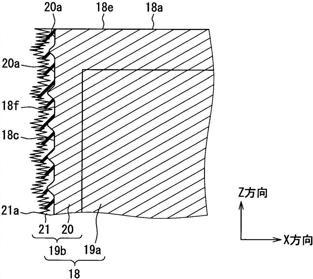
[0106] The present inventors confirmed the relationship between the presence or absence of the uneven oxide film 21 and the formation range of the uneven oxide film 21 and solder wetting. express its results in Figure 9 middle. At this time, the semiconductor device 10 was formed by the above-mentioned manufacturing method and evaluated. When there is no uneven oxide film 21, the amount of the second solder 22 that does not cause wetting and spreading to the joint 18 was used as a reference amount, and a comparison was made between the reference amount and the amount three times the reference amount. In addition, the formation range of the uneven oxide film 21 on the side surface 18c is set to the entire surface, from the end on the first opposing surface 18a side to 1 / 2 of the side surface 18c, and from the first opposing surface 18a side. These three types from the end up to 1 / 3 of the side 18c were compared. At this time, using an energy density of 12J / cm 2 Concavo-con...

Embodiment 2

[0111] The present inventors confirmed the relationship between the presence or absence of the metal thin film 20 , the type of the metal thin film 20 , the presence or absence of the uneven oxide film 21 , and the easiness of occurrence of solder bridges. express its results in Figure 10 middle. At this time, the semiconductor device 10 was formed by the above-mentioned manufacturing method and evaluated. That is, in the case of forming the uneven oxide film 21, at an energy density of 6 J / cm 2 The metal thin film 20 was irradiated with laser light, and then soldered by reduced-pressure reflow under a hydrogen atmosphere. Regarding the metal thin film 20 , the metal thin film 20 formed by electroplating Ni and the metal thin film 20 formed by electroless Ni plating were respectively evaluated.

[0112] In addition, in each case, the material tolerance target value (hereinafter, expressed as material tolerance Typ) and the material tolerance max were evaluated. The materi...


PUM

PropertyMeasurementUnit
Diameteraaaaaaaaaa

Abstract

A semiconductor device is provided with: a semiconductor chip (11, 11H, 11L) having an electrode (12) on one surface (11a); a first conductive member (23, 23H, 23L) on the one surface side of the semiconductor chip; a metal member (18, 18H, 18L), which has a base material (19a) and a film (19b), and is disposed between the semiconductor chip and the first conductive member; a first solder (17) between the metal member and the electrode of the semiconductor chip; and a second solder (22) between the metal member and the first conductive member. The film has, on the front surface of the base material, a metal thin film (20) and a recessed and protruding oxide film (21, 31, 32). The recessed and protruding oxide film is disposed on the metal thin film in a part of a connection region (18f) that connects to each other a first connection region (18d) having the first solder connected thereto, and a second connection region (18e) having the second solder connected thereto, said part being a part of the front surface of the metal member.

Description

[0001] Cross-reference of related applications [0002] This application is based on Japanese Patent Application No. 2014-250186 filed on December 10, 2014, Japanese Patent Application No. 2015-99403 filed on May 14, 2015, and Japanese Patent Application filed on November 13, 2015 No. 2015-223330, the content of which is quoted here. technical field [0003] This disclosure relates to a semiconductor chip in which a first conductive member is disposed via a metal member on one side of a semiconductor chip, electrodes formed on one side are connected to the metal member by a first solder, and the metal member and the first conductive member are connected by a second solder. Device and method for its manufacture. Background technique [0004] For example, as shown in Patent Document 1, it is known that a first conductive member (second metal plate) is arranged on one side of a semiconductor chip (semiconductor element) via a metal member (bulk), and electrodes formed on one s...

Claims


Application Information

Patent Timeline
IPC IPC(8): H01L23/48H01L23/40
CPCH01L2924/181H01L2224/33H01L23/3107H01L23/4334H01L23/488H01L23/49562H01L23/49575H01L2224/26175H01L23/3142H01L25/0655H01L25/50H01L2224/2612H01L2924/00012H01L21/4825H01L21/565H01L23/293H01L23/4952H01L23/49527
Inventor 林英二小林涉野村英司神田和辉
Owner DENSO CORP
Why Eureka
Try Eureka