Graphene/bilayer tellurene/borene van der Waals heterojunction photodiode device

A photodiode and heterojunction technology, applied in electrical components, semiconductor devices, circuits, etc., can solve the problem of inability to combine high light detection rate and high light responsivity, and achieve the effect of enhancing rectification effect and enhancing light absorption intensity.

Active Publication Date: 2022-07-12
JIAXING UNIV
View PDF4 Cites 0 Cited by
  • Summary
  • Abstract
  • Description
  • Claims
  • Application Information

AI Technical Summary

Problems solved by technology

[0005] In order to solve the above-mentioned problems in the prior art, the present invention provides a double-layer tellurene / borene van der Waals heterojunction photodiode device structure with both high photodetection rate and high photoresponsivity, which solves the problem that photodiode devices in the prior art cannot combine Problems with high photodetectivity and high photoresponsivity

Method used


Image

  • Graphene/bilayer tellurene/borene van der Waals heterojunction photodiode device
  • Graphene/bilayer tellurene/borene van der Waals heterojunction photodiode device
  • Graphene/bilayer tellurene/borene van der Waals heterojunction photodiode device

Examples


Embodiment 1

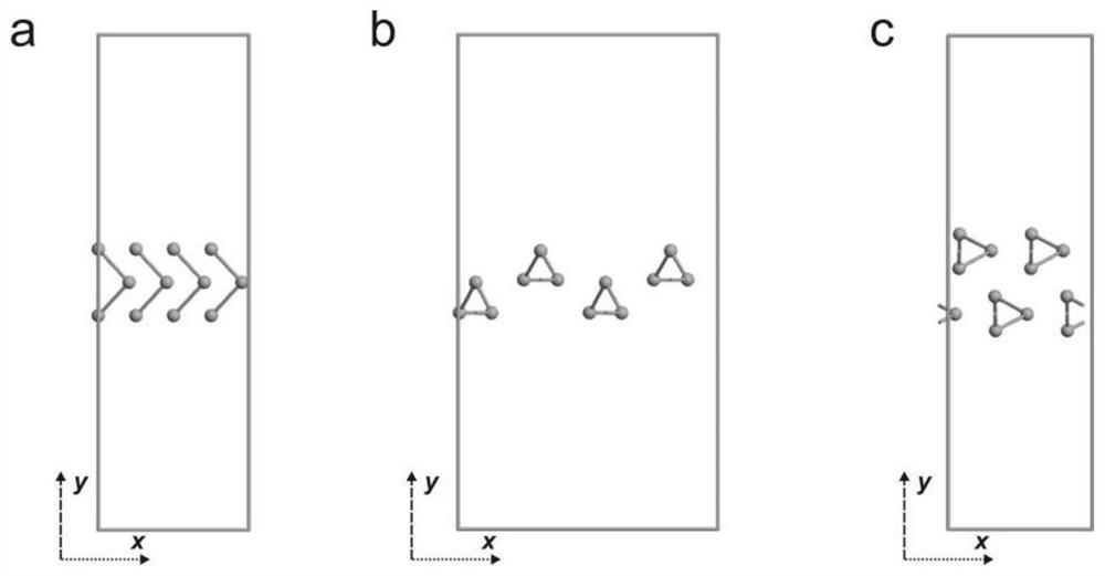
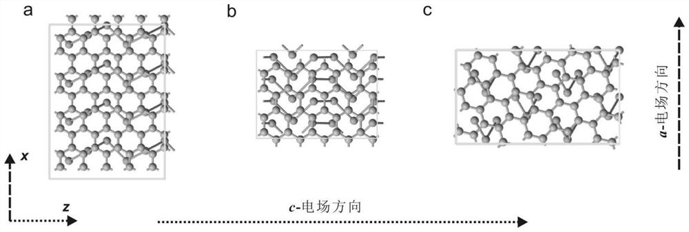
[0054] A graphene / double-layer tellurene / borene van der Waals heterojunction photodiode device with a vacuum layer thickness of like figure 1 (b), shown in 10, it is composed of single-layer graphene 1, double-layer tellurene 2 and single-layer borophene 4; the structure of double-layer tellurene belongs to α crystal type, and its crystal lattice orientation is [010] crystal direction;

[0055] The horizontal electric field c-direction coplanar with the bilayer tellurene (the horizontal electric field c-direction is the direction of the electric field applied horizontally along the z-direction of the coordinate axis of the van der Waals heterocrystal cell) is the horizontal direction D, along the horizontal direction D, The bilayer tellurene is composed of m1, m2 and m3 segments from left to right, and the single-layer borophene is composed of n1, n2 and n3 segments from left to right; single-layer graphene and m1 segment form the left electrode region, The length of m2, m3...

Embodiment 2

[0060] A graphene / double-layer tellurene / borene van der Waals heterojunction photodiode device with a vacuum layer thickness of like Figure 11 As shown, it is composed of single-layer graphene 1, double-layer tellurene 2 and single-layer borophene 4; the structure of double-layer tellurene belongs to α crystal type, and its lattice orientation is [010] crystal direction;

[0061] The horizontal electric field a-direction coplanar with the bilayer tellurene (the horizontal electric field a-direction is the direction of the horizontally applied electric field along the x-direction of the coordinate axis of the van der Waals heterocrystal cell) is the horizontal direction D, along the horizontal direction D, The bilayer tellurene is composed of m1, m2 and m3 segments from left to right, and the single-layer borophene is composed of n1, n2 and n3 segments from left to right; single-layer graphene and m1 segment form the left electrode region, The length of m2, m3, n1 and n2 is ...

Embodiment 3

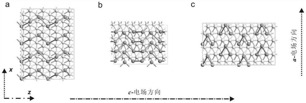
[0066] A graphene / double-layer tellurene / borene van der Waals heterojunction photodiode device with a vacuum layer thickness of like figure 1 As shown in (c) and 12, it is composed of single-layer graphene 1, double-layer tellurene 2 and single-layer borophene 4; the structure of double-layer tellurene belongs to α crystal type, and its lattice orientation is [100] crystal direction;

[0067] The horizontal electric field c-direction coplanar with the bilayer tellurene (the horizontal electric field c-direction is the direction of the electric field applied horizontally along the z-direction of the coordinate axis of the van der Waals heterocrystal cell) is the horizontal direction D, along the horizontal direction D, The bilayer tellurene is composed of m1, m2 and m3 segments from left to right, and the single-layer borophene is composed of n1, n2 and n3 segments from left to right; single-layer graphene and m1 segment form the left electrode region, The length of m2, m3, ...


PUM


Abstract

The invention relates to a graphene / double-layer tellurene / borene van der Waals heterojunction photodiode device, which is composed of single-layer graphene, double-layer tellurene and single-layer borophene; From left to right, it consists of m1 segment, m2 segment and m3 segment. From left to right, single-layer boronene consists of n1 segment, n2 segment and n3 segment; single-layer graphene and m1 segment form the left electrode area, and m2 segment and m3 segment , n1 and n2 segments constitute the central scattering region, and n3 segment constitutes the right electrode region; the single-layer graphene is vertically stacked on the m1 segment along the horizontal direction D to form a graphene / double-layer tellurene van der Waals heterojunction; the m3 segment is along the horizontal direction D stacking vertically on the n1 segment forms a bilayer tellurene / borene van der Waals heterojunction. The invention utilizes the lattice orientation of the double-layer tellurene and the direction of the horizontally applied electric field to regulate the lateral Schottky potential barrier between the left electrode and the center scattering region, enhance the rectification effect of the photodiode, and obtain a simple and efficient device with both high light detection rate and high light detection rate. Heterojunction photodiodes with high photoresponsivity.

Description

technical field [0001] The invention relates to the technical field of semiconductors, in particular to a photodiode device structure using structural anisotropy to improve a double-layer tellurene / borene van der Waals heterojunction with both high light detection rate and high light responsivity. Background technique [0002] The increasing miniaturization of next-generation electronic optoelectronic devices is accompanied by the requirement to overcome short-channel effects, necessitating the exploration of novel device structures. Taking two-dimensional van der Waals heterojunctions as an example, van der Waals integration is the physical assembly of synthesized structural units through van der Waals interactions, providing a low-energy integration method that is not affected by lattice and process constraints. limit. The optoelectronic properties of 2D materials can be tuned by van der Waals integration, making van der Waals heterojunctions promising for optoelectronic ...

Claims


Application Information

Patent Timeline
Patent Type & Authority Patents(China)
IPC IPC(8): H01L31/0352H01L31/0296H01L31/028H01L31/0256
CPCH01L31/0352H01L31/035272H01L31/0256H01L31/0296H01L31/028H01L2031/0344Y02P70/50
Inventor 贺园园程娜赵健伟
Owner JIAXING UNIV
Why Eureka
Try Eureka