Superlattice layer, LED epitaxial structure, display device and manufacturing method of LED epitaxial structure

A technology of superlattice layer and epitaxial structure, applied in electrical components, nanotechnology, circuits, etc., can solve problems such as lattice mismatch, n-type doped gallium nitride layer shift, and affect luminous characteristics, etc., reaching V Effects of reducing type defects, ensuring luminous performance, and reducing dislocations

Active Publication Date: 2021-09-28
CHONGQING KONKA PHOTOELECTRIC TECH RES INST CO LTD
View PDF7 Cites 0 Cited by
  • Summary
  • Abstract
  • Description
  • Claims
  • Application Information

AI Technical Summary

Problems solved by technology

[0003] The existing blue LED epitaxial structure is mainly to sequentially grow gallium nitride (GaN) buffer layer, non-doped gallium nitride layer, n-type doped gallium nitride layer and other structures on the sapphire substrate, and make LED devices; but Because there is a large lattice mismatch between gallium nitride and sapphire; wherein, the lattice mismatch refers to the mismatch phenomenon caused by the difference in lattice constant between the substrate and the epitaxial layer; and in the existing LED During the growth process of the epitaxial structure, the n-type doped gallium nitride layer is generated at one time, so the stress generated during the growth is relatively large, so that the n-type doped gallium nitride layer will occur under the action of stress. Displacement, resulting in a large dislocation between the n-type doped GaN layer and the substrate, and its threading dislocation will reach the multiple quantum well (multiplequantum well, MQW) region to form a V-type defect, thereby affecting its luminescence characteristic

Method used


Image

  • Superlattice layer, LED epitaxial structure, display device and manufacturing method of LED epitaxial structure
  • Superlattice layer, LED epitaxial structure, display device and manufacturing method of LED epitaxial structure
  • Superlattice layer, LED epitaxial structure, display device and manufacturing method of LED epitaxial structure

Examples


Embodiment Construction

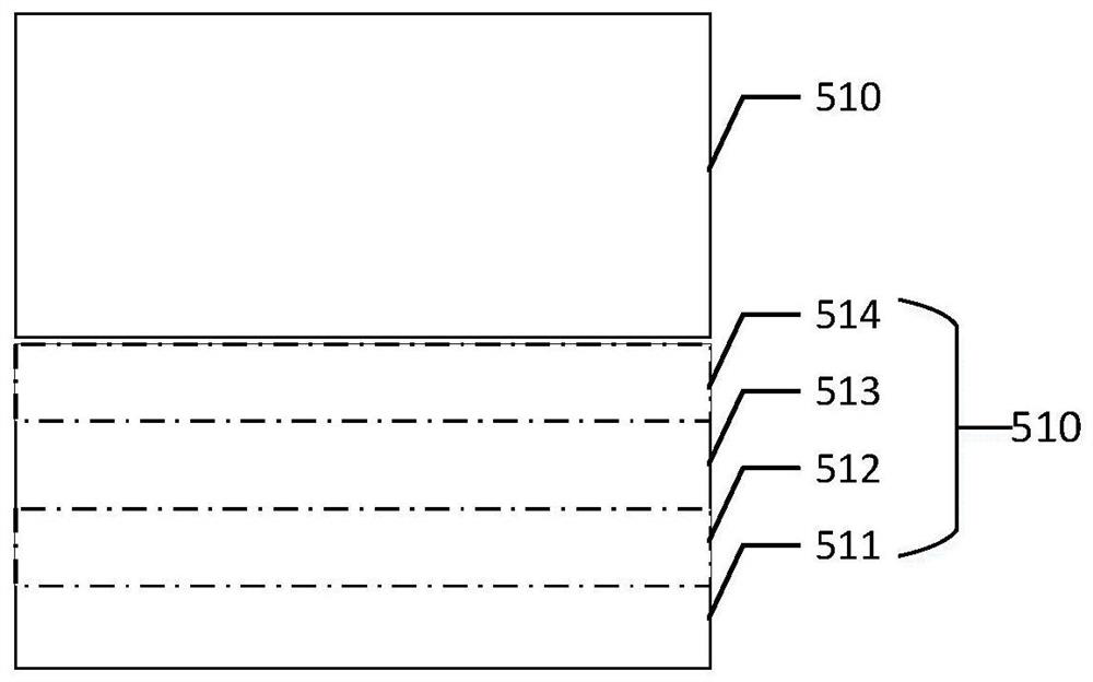
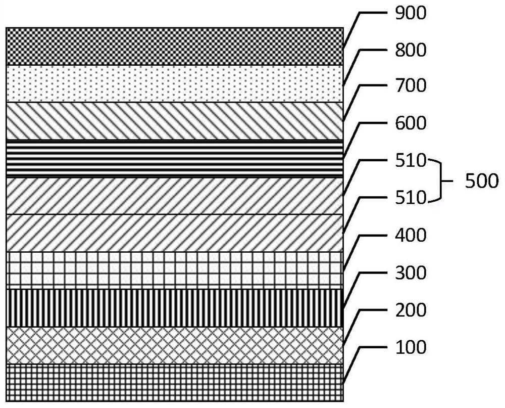
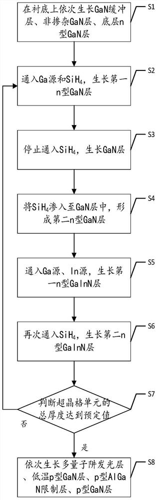
[0038] In order to make the object, technical solution and advantages of the present invention more clear, the present invention will be further described in detail below in conjunction with the accompanying drawings and embodiments. It should be understood that the specific embodiments described here are only used to explain the present invention, not to limit the present invention.

[0039] In describing the present invention, it should be understood that the terms "center", "longitudinal", "transverse", "length", "width", "thickness", "upper", "lower", "front", " Orientation indicated by rear, left, right, vertical, horizontal, top, bottom, inside, outside, clockwise, counterclockwise, etc. The positional relationship is based on the orientation or positional relationship shown in the drawings, which is only for the convenience of describing the present invention and simplifying the description, rather than indicating or implying that the referred device or element must hav...


PUM

PropertyMeasurementUnit
thicknessaaaaaaaaaa
thicknessaaaaaaaaaa
thicknessaaaaaaaaaa

Abstract

The invention relates to the technical field of light-emitting diodes, and in particular, relates to a superlattice structure, an LED epitaxial structure, a display device and a production method of the LED epitaxial structure. The superlattice structure comprises at least two superlattice cells growing successively in a stacked manner; each superlattice unit comprises a first n-type GaN layer, a second n-type GaN layer, a first n-type GaInN layer and a second n-type GaInN layer which are sequentially stacked and grown, wherein the doping concentration of the first n-type GaN layer in the growth direction is fixed, the doping concentration of the second n-type GaN layer in the growth direction is gradually increased, the doping concentration of the first n-type GaInN layer in the growth direction is gradually reduced, and the doping concentration of the second n-type GaInN layer in the growth direction is fixed; and the stress in the epitaxial structure can be effectively released in the production process, so that dislocation between the n-type GaN layer and the substrate caused by the action of the stress can be reduced, and the light-emitting performance of the LED is effectively ensured.

Description

technical field [0001] The present invention relates to the technical field of light-emitting diodes, in particular to a superlattice layer, an LED epitaxial structure with the superlattice layer, a display device with the LED epitaxial structure, and a method for the superlattice layer. A production method and a method for manufacturing the LED epitaxial structure. Background technique [0002] With the development of science and technology, light-emitting diodes (Light Emitting Diode, LED) are widely used due to their good stability, lifespan, low power consumption, color saturation, fast response, and strong contrast. used in display devices. Existing LED chips all contain LED epitaxial structure, and LED epitaxial structure refers to a specific single crystal thin film grown on a substrate heated to an appropriate temperature. The substrate material of LED epitaxial structure is the cornerstone of the development of LED technology; the substrate material determines the...

Claims


Application Information

Patent Timeline
Patent Type & Authority Applications(China)
IPC IPC(8): H01L33/04H01L33/12H01L33/00B82Y30/00B82Y40/00
CPCH01L33/04H01L33/12H01L33/007B82Y30/00B82Y40/00H01L33/00H01L33/06H01L33/32
Inventor 黄文洋林雅雯黄国栋黄嘉宏杨顺贵
Owner CHONGQING KONKA PHOTOELECTRIC TECH RES INST CO LTD
Why Eureka
Try Eureka