Aliasing electronic component space expression method based on improved monocular depth estimation
A technology for electronic components and depth estimation, applied in computer components, neural learning methods, instruments, etc., to achieve the effect of solving aliasing electronic components, improving speed, and ensuring comprehensiveness
- Summary
- Abstract
- Description
- Claims
- Application Information
AI Technical Summary
Problems solved by technology
Method used
Image
Examples
Embodiment Construction
[0031] Embodiments of the present invention are described in detail below, examples of which are shown in the drawings, wherein the same or similar reference numerals designate the same or similar elements or elements having the same or similar functions throughout. The embodiments described below by referring to the figures are exemplary and are intended to explain the present invention and should not be construed as limiting the present invention.
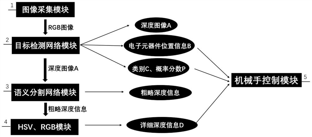
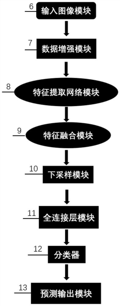
[0032] Use the camera to collect images of different types of aliased electronic components in the material box to obtain RGB images of electronic components; each image is randomly scaled twice and cut randomly twice; using the lightweight algorithm in target detection and deep convolution algorithm to extract features from the processed image; fuse the extracted shallow features and deep features; after downsampling, fully connected layer, and classifier, the depth image, electronic component position information, and electronic...
PUM
 Abstract
Description
Claims
Application Information
 - R&D
- Intellectual Property
- Life Sciences
- Materials
- Tech Scout
- Unparalleled Data Quality
- Higher Quality Content
- 60% Fewer Hallucinations
Browse by: Latest US Patents, China's latest patents, Technical Efficacy Thesaurus, Application Domain, Technology Topic, Popular Technical Reports.
© 2025 PatSnap. All rights reserved.Legal|Privacy policy|Modern Slavery Act Transparency Statement|Sitemap|About US| Contact US: help@patsnap.com


