
A high cleanliness semiconductor wafer automatic loading equipment

An automatic loading and high-cleanliness technology, which is applied in semiconductor/solid-state device manufacturing, transportation and packaging, electrical components, etc., can solve the problems of many manual operations, low automation, and many wafer contacts, so as to save labor, The effect of high degree of automation

Active Publication Date: 2021-11-02
南通煜米激光科技有限公司
View PDF6 Cites 2 Cited by
  • Summary
  • Abstract
  • Description
  • Claims
  • Application Information

AI Technical Summary

Problems solved by technology

[0005] The object of the present invention is to provide a high-cleanliness semiconductor wafer automatic loading equipment, which solves the problem that the current loading equipment in the background technology has a low degree of automation and a lot of manual operations during the working process, which leads to the relatively low contact between the wafer and the outside world. There are many, thus affecting the overall quality of the wafer. Secondly, in the production process, some wafers have defects and are difficult to be found, resulting in damaged wafers being packaged and used, which affects the quality of later use.

Method used


Image

  • A high cleanliness semiconductor wafer automatic loading equipment
  • A high cleanliness semiconductor wafer automatic loading equipment
  • A high cleanliness semiconductor wafer automatic loading equipment

Examples


Embodiment Construction

[0033] The following will clearly and completely describe the technical solutions in the embodiments of the present invention with reference to the accompanying drawings in the embodiments of the present invention. Obviously, the described embodiments are only some, not all, embodiments of the present invention. Based on the embodiments of the present invention, all other embodiments obtained by persons of ordinary skill in the art without making creative efforts belong to the protection scope of the present invention.

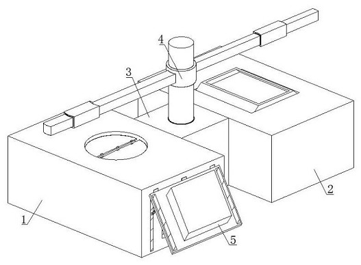
[0034] refer to Figure 1-3 , a high-cleanliness semiconductor wafer automatic loading equipment, comprising a mechanical and electrical box 3, a main box 1 arranged on one side of the electromechanical box 3, and a sub-box 2 arranged on the other side of the electromechanical box 3, and the body of the electromechanical box 3 The upper end is provided with a pick-up mechanism 4, one side of the main box body 1 is provided with a closing mechanism 5 and a conv...


PUM


Abstract

The invention relates to the field of semiconductor technology, and discloses a high-cleanliness semiconductor wafer automatic loading device, which includes an electromechanical box, a main box arranged on one side of the electromechanical box, and a sub-box arranged on the other side of the electromechanical box. The upper end of the box is provided with a pick-up mechanism, one side of the main box is provided with a closing mechanism and a conveying mechanism, one end of the conveying mechanism is connected with the inner wall of the main box, the inside of the main box is provided with a lifting mechanism, and the side of the auxiliary box is There is a lifting mechanism inside. Use the extension of the main telescopic rod to place the splint on both sides of the loading box group, and then use the lifting rod to lift the loading box group upwards. When it moves to the elastic opening, attach the electromagnet The same magnetism will generate a repulsive force, which will separate the two sets of splints, so that the loading box set will move upwards and pass through the elastic opening, and the elastic opening can only pass through from bottom to top, so as to realize the loading preparation of the loading box set , and the degree of automation is high, saving labor.

Description

technical field [0001] The invention relates to the technical field of semiconductors, in particular to an automatic loading device for high-cleanness semiconductor wafers. Background technique [0002] Wafer refers to the silicon wafer used to make silicon semiconductor circuits. Its raw material is silicon. High-purity polysilicon is dissolved and mixed with silicon crystal seeds, and then slowly pulled out to form cylindrical monocrystalline silicon. After grinding, polishing, and slicing, silicon wafers are formed, that is, wafers. At present, domestic wafer production lines are mainly 8-inch and 12-inch. [0003] After the wafer is produced, it needs to be loaded. The current loading equipment has a low degree of automation and more manual operations during the working process, which leads to more contact between the wafer and the outside world, which affects the overall quality of the wafer. Secondly, in the production process, some wafers have defects and are diffic...

Claims


Application Information

Patent Timeline
Patent Type & Authority Patents(China)
IPC IPC(8): H01L21/677H01L21/67
CPCH01L21/67742H01L21/67766H01L21/67769H01L21/67778H01L21/67288
Inventor 詹华贵
Owner 南通煜米激光科技有限公司
Features
  • Generate Ideas
  • Intellectual Property
  • Life Sciences
  • Materials
  • Tech Scout
  • Unparalleled Data Quality
  • Higher Quality Content
  • 60% Fewer Hallucinations
Learn More