Chip ball mounting method

A chip and ball planting technology, which is applied in the manufacture of electrical components, electrical solid devices, semiconductor/solid devices, etc., can solve problems such as long working time and low success rate

Pending Publication Date: 2021-10-12
HITECH SEMICON WUXI
View PDF1 Cites 0 Cited by
  • Summary
  • Abstract
  • Description
  • Claims
  • Application Information

AI Technical Summary

Problems solved by technology

The existing ball planting method is to manually place the solder balls at the required points. The success rate of this method is too low and the operation time is too long

Method used


Image

  • Chip ball mounting method
  • Chip ball mounting method
  • Chip ball mounting method

Examples


Embodiment Construction

[0021] The utility model will be described in detail below in conjunction with the accompanying drawings. The description in this part is only exemplary and explanatory, and should not have any limiting effect on the protection scope of the present invention.

[0022] The invention provides a chip ball planting method, comprising the following steps:

[0023] S1: Use copper fiber heat conduction and organic flux to remove the original solder balls;

[0024] S2: The shape of the solder balls picked after reflow soldering may be different. To ensure the convenience of subsequent operations, remove all the solder balls on the substrate to restore the flatness of the substrate;

[0025] S3: Use jigs to distribute solder balls;

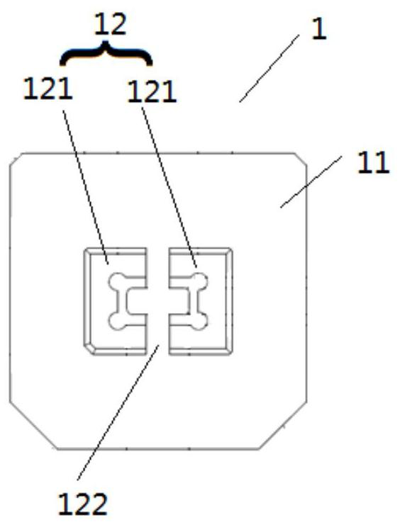
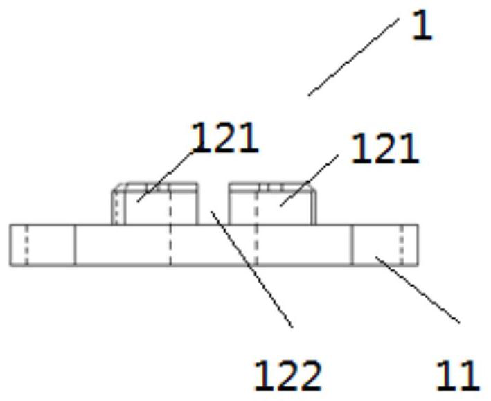
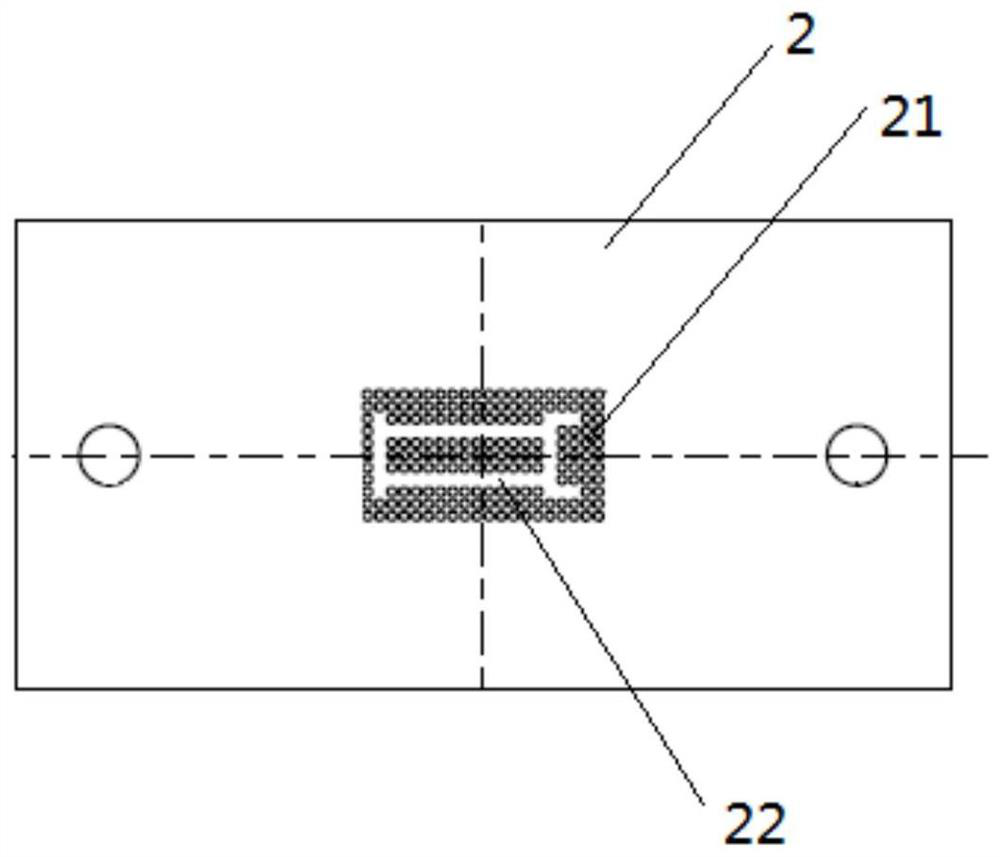
[0026] A planting device, comprising: a base 1 and a grid top plate 2;

[0027] The base 1 includes a bottom plate 11 and a placement platform 12, the placement platform 12 is arranged on the bottom plate 11; the placement platform 12 includes a protrusi...


PUM


Abstract

The purpose of the invention is to provide a chip ball mounting method. In the process of removing solder balls, copper fiber heat conduction is adopted to be matched with organic soldering flux, and the solder balls can be uniformly heated and melted and adsorbed to the copper fiber. The chip ball mounting method comprises the following steps: S1, removing original solder balls by adopting copper fiber heat conduction in cooperation with an organic soldering flux; S2, removing all the solder balls on the substrate, so that the substrate is recovered to be flat; S3, performing solder ball distribution by using a jig; S4, using a low-temperature heating table for heating and melting, and then welding the solder balls to the chip. The method has the beneficial effects that in the solder ball removing process, copper fiber heat conduction is adopted to be matched with organic scaling powder, and the solder balls can be evenly heated and melted and adsorbed to the copper fiber.

Description

technical field [0001] The present invention relates to chip ball planting technology, specifically a chip ball planting method. Background technique [0002] The fine-pitch ball grid array chips (hereinafter referred to as chips) produced today have no stable and effective way to reball when faced with disassembly analysis or maintenance. Since the chip ball disassembled from the module is no longer complete, it needs to be re-planted to resume use. The existing ball planting method is to manually place the solder balls at the required points. The success rate of this method is too low and the operation time is too long. [0003] A Chinese utility model patent has been published, publication number: CN103855041B, patent name: a chip ball planting device and method, application date: 20121206, which discloses a chip ball planting device and method, the chip ball planting device includes: an upper shell body, stencil and lower shell; the lower shell is provided with a shell...

Claims


Application Information

Patent Timeline
Patent Type & Authority Applications(China)
IPC IPC(8): H01L21/60
CPCH01L24/11H01L24/742H01L2224/742H01L2224/11848
Inventor 赵腾俊刘欣
Owner HITECH SEMICON WUXI
Why Eureka
Try Eureka