Method for processing local dead pixels of superconducting tape in high-temperature superconducting narrow pile line
A technology of high-temperature superconducting tapes and superconducting tapes, applied in the usage of superconducting elements, superconducting/high-conducting conductors, superconducting devices, etc., to achieve the effect of reducing power transmission efficiency and increasing energy loss
- Summary
- Abstract
- Description
- Claims
- Application Information
AI Technical Summary
Problems solved by technology
Method used
Image
Examples
Embodiment 1
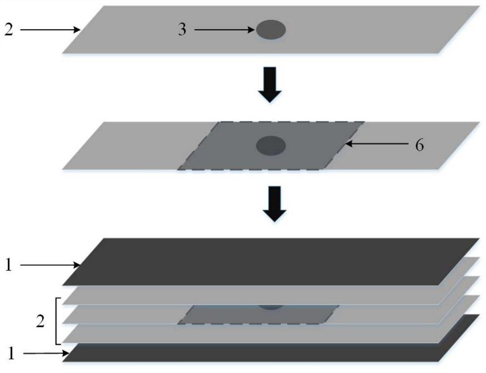
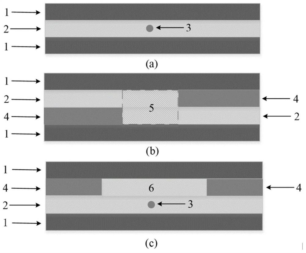
[0040] This embodiment provides a method for processing local dead spots of superconducting strips in a high-temperature superconducting narrow stack line; figure 1 is a process flow chart, wherein, the local dead spot 3 is located on the second-generation high-temperature superconducting strip 2 to be tested, and the second-generation high-temperature superconducting strip sample is attached to the local bad spot of the second-generation high-temperature superconducting strip 2 to be tested. At point 3, the second-generation high-temperature superconducting strip 2 to be tested is located between the red copper strip 1 and the red copper strip 1, and the second-generation high-temperature superconducting strip 2 to be tested attached to the second-generation high-temperature superconducting strip sample is stacked After encapsulation, a superconducting interlayer 6 is formed.
[0041] The specific method is as follows:
[0042] Prepare narrow stack wire materials: the second...
Embodiment 2
[0047] Prepare narrow stack wire materials: the second-generation high-temperature superconducting tape to be tested 2, the second-generation high-temperature superconducting tape sample, and the copper tape 1.
[0048] S1, measure the critical current of the second-generation high-temperature superconducting strip 2 to be tested, the critical current Ic decays from the original 70A to the area of local dead spots 3 at 10A, and the length of this dead spot area is 10mm; the width is 2mm.
[0049] S2. Face-to-face attachment of superconducting tape: select a second-generation high-temperature superconducting tape sample with a length of 20 mm and a width of 2 mm, and attach the selected second-generation high-temperature superconducting tape sample to the surface by diffusion pressing in a face-to-face manner. The dead point area of the second-generation high-temperature superconducting strip 2 to be tested. The fabrication of the diffusion press joint is the same as in Ex...
Embodiment 3
[0052] Prepare narrow stack wire materials: the second-generation high-temperature superconducting tape to be tested 2, the second-generation high-temperature superconducting tape sample, and the copper tape 1.
[0053] S1. Measure the critical current at each place of the second-generation high-temperature superconducting strip 2 to be tested. The critical current Ic has decayed from the original 70A to the area of local bad spots 3 at 10A. The length of the dead spot area is 18.18mm; the width is 2mm.
[0054] S2. Face-to-face attachment of superconducting tape: select a second-generation high-temperature superconducting tape sample with a length of 20 mm and a width of 2 mm, and attach the selected second-generation high-temperature superconducting tape sample to the surface by diffusion pressing in a face-to-face manner. The dead point area of the second-generation high-temperature superconducting strip 2 to be tested. The fabrication of the diffusion press joint is t...
PUM
| Property | Measurement | Unit |
|---|---|---|
| width | aaaaa | aaaaa |
Abstract
Description
Claims
Application Information


