Generative adversarial network and computer-generated holography-based chip defect detection method

A computational holography and detection method technology, applied in computing, computer parts, character and pattern recognition, etc., can solve the problems of imperfect imaging technology, slow detection speed, weak generalization ability, etc., to reduce the impact of environmental factors and practical Cost, effect of solving 3D modeling and imaging problems, improving accuracy and generalization ability

Pending Publication Date: 2021-10-26
XIDIAN UNIV
View PDF0 Cites 0 Cited by
  • Summary
  • Abstract
  • Description
  • Claims
  • Application Information

AI Technical Summary

Problems solved by technology

At the same time, miniaturized chips require 3D modeling and imaging to achieve precise size measurement and appearance inspection, and the current imaging technology is n

Method used


Image

  • Generative adversarial network and computer-generated holography-based chip defect detection method
  • Generative adversarial network and computer-generated holography-based chip defect detection method
  • Generative adversarial network and computer-generated holography-based chip defect detection method

Examples


Embodiment Construction

[0035] In order to make the object, technical solution and advantages of the present invention clearer, the present invention will be further described in detail below in conjunction with the accompanying drawings and embodiments. It should be understood that the specific embodiments described here are only used to explain the present invention, not to limit the present invention.

[0036] The specific implementation of the present invention will be described in detail below in conjunction with specific embodiments.

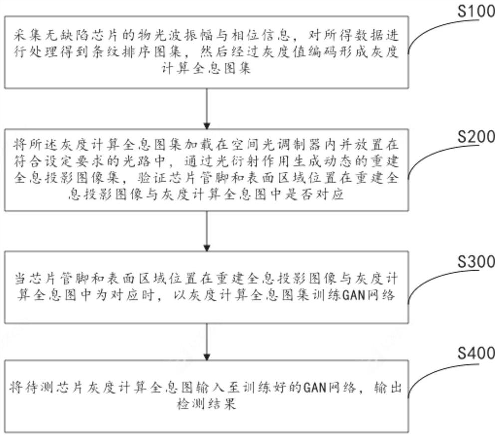
[0037] like figure 1 As shown, a chip defect detection method based on generative adversarial network and computational holography provided by an embodiment of the present invention includes the following steps:

[0038] S100, collecting the object light wave amplitude and phase information of the defect-free chip, processing the obtained data to obtain a fringe sorting atlas, and then forming a gray-scale calculation holographic atlas through gray-scale value e...


PUM


Abstract

The invention is suitable for the technical field of chip defect detection, and provides a generative adversarial network and computer-generated holography-based chip defect detection method, which comprises the following steps of: collecting object light wave amplitude and phase information of a defect-free chip, processing the obtained data to obtain a fringe sorting diagram, then forming a gray-scale computer-generated hologram through gray-scale value coding; loading the gray-scale computer-generated hologram in a spatial light modulator, placing the spatial light modulator in a light path meeting a set requirement, and generating a dynamic reconstructed holographic projection image through a light diffraction effect; training the GAN network by using the gray-scale computer-generated hologram; and inputting the gray scale computer-generated hologram of the to-be-detected chip into the trained GAN network, and outputting a detection result. The method has the beneficial effects that the problems of 3D modeling and imaging of the miniaturized chip are solved, the influence of environmental factors and the actual cost in the optical process are reduced, and the chip detection is relatively high in detection speed.

Description

technical field [0001] The invention relates to the technical field of chip defect detection, in particular to a chip defect detection method based on generative confrontation network and computational holography. Background technique [0002] With the rapid development of various high-tech fields such as military industry and aerospace, the demand for high-quality and high-reliability chips is more urgent. Therefore, the secondary screening of factory chips is particularly important. Chip electrical performance and other tests in the secondary screening are necessary prerequisites for chip quality assurance. At the same time, the detection of chip appearance defects such as chip marking, surface integrity, chip pins, chip size, etc. also play a big role in the reliability of the chip. Impact. At present, the third-party screening manufacturers of chips still adopt the traditional manual visual inspection method in the field of chip appearance defect detection, which requi...

Claims


Application Information

Patent Timeline
IPC IPC(8): G06T7/00G06K9/62G06T7/49
CPCG06T7/0004G06T7/49G06T2207/20081G06T2207/30148G06T2207/10024G06F18/241
Inventor 任获荣党翔宇刘君荣孙璐吕银飞徐思宇
Owner XIDIAN UNIV
Why Eureka
Try Eureka