Mach-Zehnder interferometer using photonic band gap crystals

a technology of photonic band gap crystals and interferometers, which is applied in the direction of instruments, semiconductor lasers, optical elements, etc., can solve the problems that the properties cannot be altered, and achieve the effect of small size, easy to achieve q, and large operation bandwidth

Inactive Publication Date: 2005-07-12
MASSACHUSETTS INST OF TECH
View PDF11 Cites 261 Cited by
  • Summary
  • Abstract
  • Description
  • Claims
  • Application Information

AI Technical Summary

Benefits of technology

[0007]A Mach-Zehnder interferometer is provided using specially designed line defects in photonic band gap (PBG) crystals. In the line defects in question, the carrier light has a very low group velocity, a characteristic shape of the dispersion relation, and its dispersion relation responds in a specified way to the (electrical or optical) control stimulus. The device can be used as an electrically (or optically) induced on-off switch, or a router between two different outputs. Furthermore, it can also be

Problems solved by technology

Once a device has been built, i

Method used


Image

  • Mach-Zehnder interferometer using photonic band gap crystals
  • Mach-Zehnder interferometer using photonic band gap crystals
  • Mach-Zehnder interferometer using photonic band gap crystals

Examples


Embodiment Construction

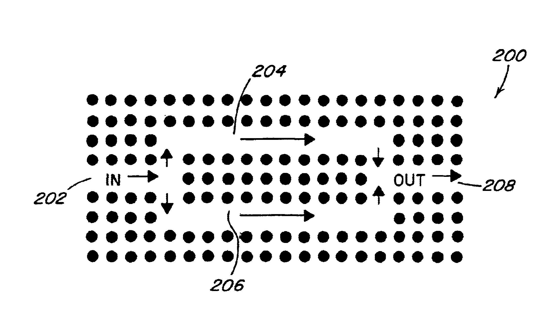
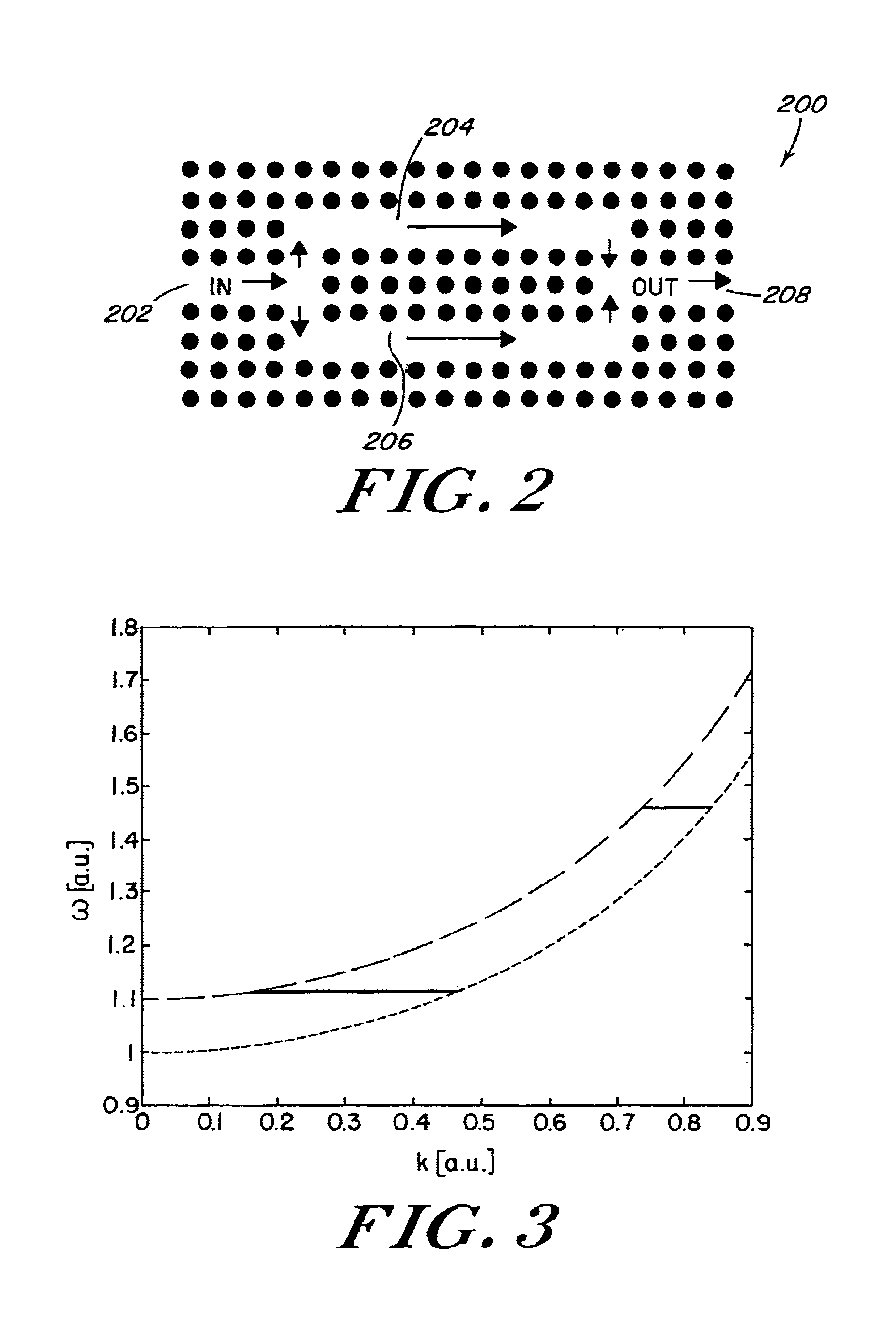
[0016]The invention provides an integrated optics device that can be used as a very fast electrically, or optically controlled switch, or else as an all-optical logical gate. The device is compared with already existing devices that have similar performance. Probably the fastest and smallest interferometers that consume the least power are either Mach-Zehnder waveguide interferometers, typically implemented in LiNbO3, directional coupler switches implemented with InGaAlAs / InAlAs multiquantum wells, or InP-based quantum-well Y-branch switches. These devices are typically O(1 mm) or longer. The invention involves a class of devices, which achieve the same performance, but with length an order of magnitude smaller. Because of the smaller size, the power needed to operate these devices is also significantly reduced. This is achieved by exploring a certain class of line defects in photonic band gap crystals.

[0017]It is desirable to configure a fast device, i.e., response time of 1 ns or ...


PUM


Abstract

A photonic crystal optical switch having a periodic dielectric structure including at least one input waveguide. First and second waveguide arms branch from the input waveguide in which the relative optical path lengths of electromagnetic radiation within the arms are controlled by stimuli. At least one output waveguide that combines the electromagnetic radiation propagating within the first and second waveguide arms.

Description

PRIORITY INFORMATION[0001]This application claims priority from provisional application Ser. No. 60 / 291,105 filed May 15, 2001.SPONSORSHIP INFORMATION[0002]This invention was made with government support under Grant No. Dmr-9808941 awarded by NSF. The government has certain rights in this invention.BACKGROUND OF THE INVENTION[0003]Photonic band gap crystals are artificially created structures in which the index of refraction is periodically modulated in 1D, 2D, or 3D, with period of modulation comparable to the wavelength of the carrier light. For a 2D example, see FIG. 1A. FIG. 1A is a schematic diagram of a 2D PBG crystal 100, in which the dark circles 102 represent regions of a high index of refraction.[0004]If the amplitude of the index variation is large enough, a photonic band gap appears, and light of certain wavelength ranges is not allowed to propagate. In many ways, PBG crystals present for photons what semiconductors present for electrons. Therefore, they are considered t...

Claims


Application Information

Patent Timeline
IPC IPC(8): G02B6/122G02F1/225H01S5/026H01S5/10
CPCB82Y20/00G02B6/1225G02F1/225G02F2202/32H01S5/0265H01S5/105H01S5/11
Inventor SOLJACIC, MARINFAN, SHANHUIIBANESCU, MIHAIJOHNSON, STEVEN G.JOANNOPOULOS, JOHN D.
Owner MASSACHUSETTS INST OF TECH
Why Eureka
Try Eureka