Wafer scribing device for machining and using method thereof

A mechanical processing and scribing technology, which is applied in the direction of electrical components, semiconductor/solid-state device manufacturing, circuits, etc., can solve the problems of increasing the work of grinding, difficult to control the scribing depth, and affecting the alignment of wafers, so as to improve efficiency , The effect of convenient alignment work

Inactive Publication Date: 2021-10-29
ZHENGZHOU UNIV OF IND TECH
View PDF0 Cites 8 Cited by
  • Summary
  • Abstract
  • Description
  • Claims
  • Application Information

AI Technical Summary

Problems solved by technology

[0002] Wafer refers to the silicon wafer used in the production of silicon semiconductor integrated circuits. Because of its circular shape, it is called a wafer. It can be processed into various circuit element structures on the silicon wafer and become an IC with specific electrical functions. Products, the raw material of the wafer is silicon, and the surface of the earth's crust is inexhaustible silica, the silica ore is refined by an electric arc furnace, chlorinated with hydrochloric acid, and distilled to produce high-purity polysilicon, wafer In the process of processing, it needs to be diced. At present, the existing wafer dicing equipment has the following shortcomings: 1. The initial placement of the wafer is relatively random, which affects the alignment of the subsequent wafers; 2. Every Only one surface of the wafer can be diced at a time, which makes it difficult to control the depth of scribing on the front and back sides, and increases the work of post-polishing

Method used


Image

  • Wafer scribing device for machining and using method thereof
  • Wafer scribing device for machining and using method thereof
  • Wafer scribing device for machining and using method thereof

Examples


Embodiment 1

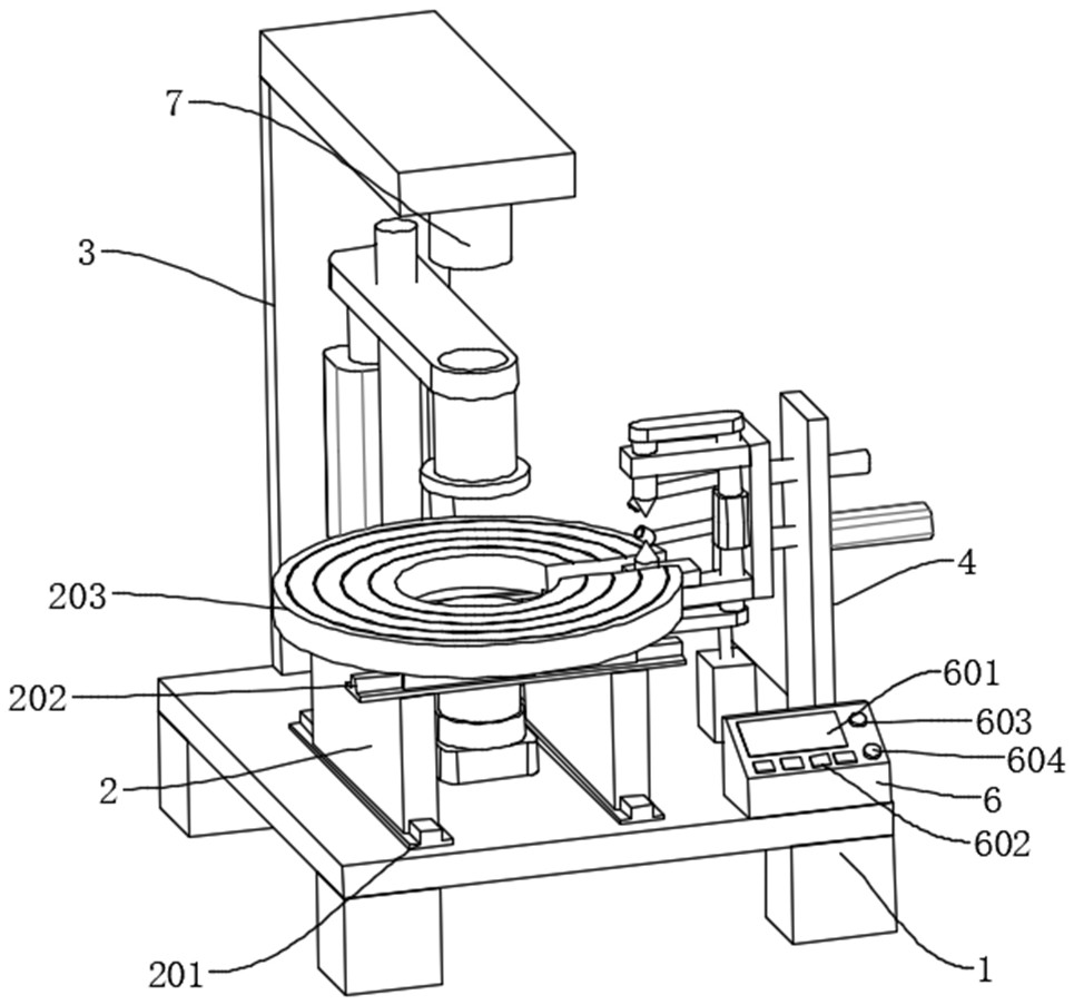
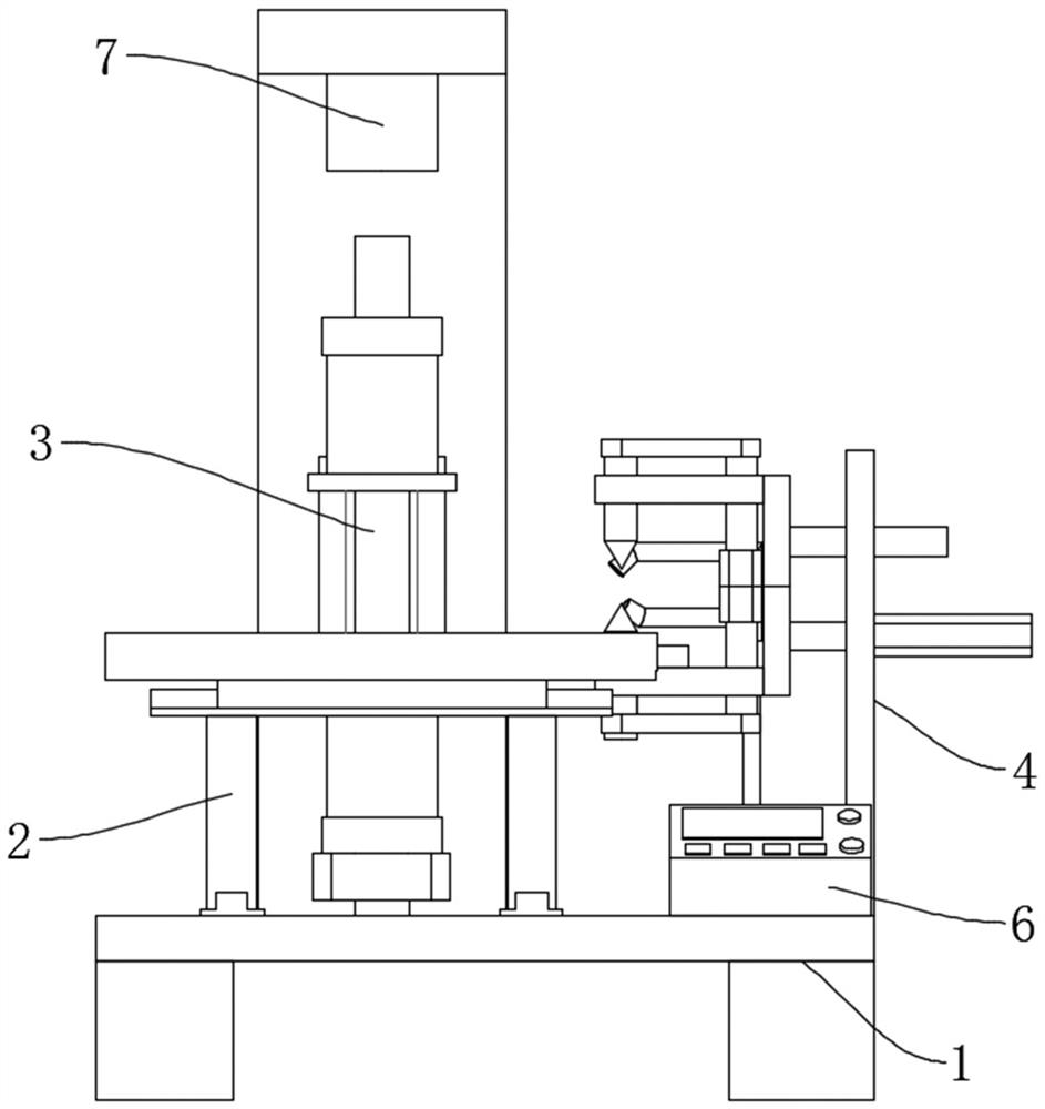
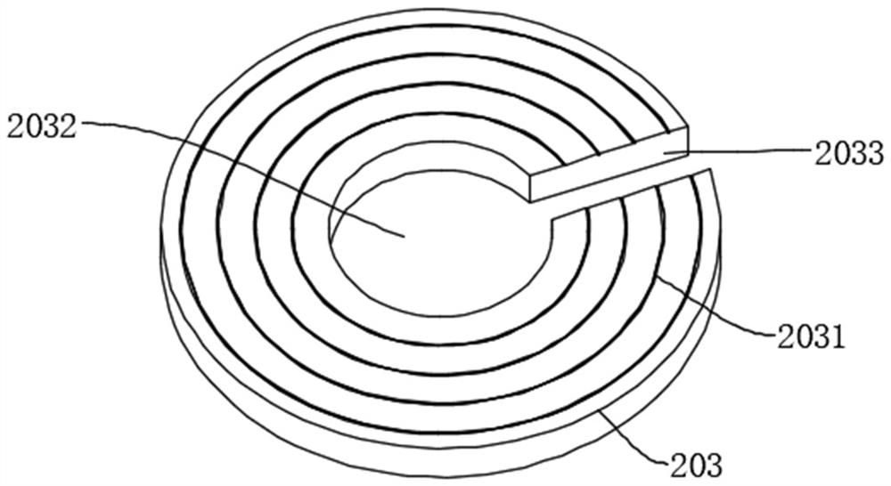
[0038] Such as Figure 1-7 As shown, a wafer dicing device for mechanical processing includes a base 1, an adjustment mechanism 2 is arranged in the center of the top of the base 1, a control panel 6 is connected to the front end side of the top of the base 1 by screws, and the adjustment mechanism 2 includes a vertical linear slide rail Pair 201, horizontal linear slide rail pair 202, placement plate 203, the top of vertical linear slide rail pair 201 is provided with horizontal linear slide rail pair 202, and the top of horizontal linear slide rail pair 202 is connected with a placement plate 203 by bolts, and the center of the top of the placement plate 203 There is a relief hole 2032, and the top of the placement plate 203 is etched with several annular scales 2031 concentric with the relief hole 2032. One side of the placement plate 203 is provided with a relief groove 2033 that runs through the placement plate 203 up and down, and the relief groove 2033 and the The relie...

Embodiment 2

[0046] Such as Figure 8As shown, the difference between Embodiment 2 and Embodiment 1 is that the scribing assembly that moves up and down synchronously includes a third support plate 405, a scribing knife 408, a positive and negative lead screw 41, an adjustment motor 42, a moving plate 43, and a third support plate 405. There are two support plates 405, and they are arranged up and down. The third support plate 405 is connected to one side of the push plate 403 by bolts, and the side of the third support plate 405 close to the push plate 403 is connected with a positive and negative lead screw 41 through a bearing. , the upper end of the positive and negative lead screw 41 passes through the third support plate 405, and the adjustment motor 42 is connected through the coupling, and the outer side of the positive and negative lead screw 41 is threaded with two moving plates 43, and the moving plate 43 is located on the two third support plates. Between the plates 405, the si...


PUM


Abstract

The invention discloses a wafer scribing device for machining and a using method thereof. The wafer scribing device comprises a base, wherein an adjusting mechanism is arranged in the center of the top of the base, a control panel is connected to one side of the front end of the top of the base through screws, the adjusting mechanism comprises a longitudinal linear sliding rail pair, a transverse linear sliding rail pair and a placement disc, and the transverse linear sliding rail pair is arranged at the top of the longitudinal linear sliding rail pair. Through transverse movement of the longitudinal linear sliding rail pair, longitudinal movement of the transverse linear sliding rail pair and cooperation with the alignment equipment body, the wafer alignment function is achieved, initial placement of wafers is facilitated through arrangement of annular scales and receding holes, and then alignment work of the wafers is facilitated; and the wafer can be fixed and driven to rotate through a clamping assembly, and a scribing assembly which moves up and down synchronously is matched to rapidly complete scribing of the two sides of the wafer, so that the scribing efficiency is improved, and it can be guaranteed that the scribing depths of the front and the back are the same.

Description

technical field [0001] The invention relates to the technical field of mechanical processing, in particular to a wafer dicing device for mechanical processing and a method for using the same. Background technique [0002] Wafer refers to the silicon wafer used in the production of silicon semiconductor integrated circuits. Because of its circular shape, it is called a wafer. It can be processed into various circuit element structures on the silicon wafer and become an IC with specific electrical functions. Products, the raw material of the wafer is silicon, and the surface of the earth's crust is inexhaustible silica, the silica ore is refined by an electric arc furnace, chlorinated with hydrochloric acid, and distilled to produce high-purity polysilicon, wafer In the process of processing, it needs to be diced. At present, the existing wafer dicing equipment has the following shortcomings: 1. The initial placement of the wafer is relatively random, which affects the alignme...

Claims


Application Information

Patent Timeline
Patent Type & Authority Applications(China)
IPC IPC(8): H01L21/67H01L21/78
CPCH01L21/67092H01L21/78
Inventor 郭光立魏德印
Owner ZHENGZHOU UNIV OF IND TECH
Why Eureka
Try Eureka