Wafer test system and method for TOF chip

A wafer testing and chip technology, which is used in radio wave measurement systems, electronic circuit testing, electrical measurement, etc., and can solve problems such as large redundancy in functions, complex hardware and software structures, and inextensibility.

Pending Publication Date: 2021-11-02
苏州芯迈智能科技有限公司
View PDF0 Cites 3 Cited by
  • Summary
  • Abstract
  • Description
  • Claims
  • Application Information

AI Technical Summary

Problems solved by technology

[0003] However, the traditional wafer testing method has problems such as large functional redundancy, high cost, poor integration, complex software and hardware structure, difficult deployment, and non-scalability.

Method used


Image

  • Wafer test system and method for TOF chip
  • Wafer test system and method for TOF chip
  • Wafer test system and method for TOF chip

Examples


Embodiment Construction

[0039] In order to make the purpose, technical solution and advantages of the present application clearer, the present application will be further described in detail below in conjunction with the accompanying drawings and embodiments. It should be understood that the specific embodiments described here are only used to explain the present application, and are not intended to limit the present application.

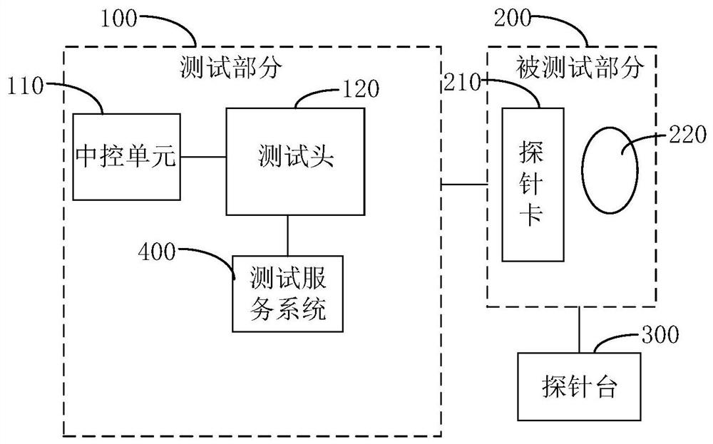
[0040] In one embodiment, such as figure 1 As shown, a wafer testing system for a TOF chip provided by the present invention mainly includes: a testing part 100, a tested part 200, and a probe station 300; wherein, the testing part 100 may include a central control unit 110 and a testing head 120; The tested part 200 may include a probe card 210 and a tested TOF chip wafer 220 .

[0041] Wherein, the probe card 210 can be connected with the probe station 300, and several contacts can be arranged on the probe card 210. Specifically, the number of contacts on the probe card...


PUM


Abstract

The invention relates to a TOF chip wafer test system and method. The system comprises a probe card, a probe station, a tested TOF chip wafer, a central control unit and a test head, wherein the probe card is provided with a plurality of contacts, and the contacts are respectively connected with different positions on the tested TOF chip wafer; board cards with different functions are respectively inserted into the clamping grooves in the testing head; the test head is used for performing a function test corresponding to the board card on the tested TOF chip wafer corresponding to each contact, and obtaining test data; and the central control unit is used for controlling the test head to work, receiving the test data transmitted from the test head, analyzing and processing the test data to obtain a test result, and transmitting the test result to the upper computer. The board cards with different functions are respectively inserted into the card slots on the test head and can be plugged according to test requirements, and multiple functions can be simultaneously tested through the same test head, so test efficiency is improved; moreover, the system reduces the equipment cost, and reduces the occupied field area of the test equipment.

Description

technical field [0001] The invention relates to the technical field of semiconductors, in particular to a TOF chip wafer testing system and method. Background technique [0002] Wafer testing is to test each die on the wafer or chip, install probes on the test head, make contact with the contacts on the die, and test its electrical characteristics. TOF (Time of Flight) technology emits an infrared light source to the object under test. After the light wave is reflected by the object, it is collected by the sensor. The system calculates the distance between the object under test and the camera by calculating the pulse difference or time difference of the received light wave. Since TOF technology is a relatively new technology, the design of TOF chips and modules is also in its infancy. Wafer testing of TOF chips is usually carried out using a CIS chip test system based on a two-dimensional image sensor chip. It is also possible to independently develop a high-speed image acq...

Claims


Application Information

Patent Timeline
Patent Type & Authority Applications(China)
IPC IPC(8): G01R31/28G01S7/497
CPCG01R31/2887G01R31/2889G01R31/2853G01S7/497
Inventor 李利民李磊穆范全
Owner 苏州芯迈智能科技有限公司
Why Eureka
Try Eureka