
Multi-channel microscope semiconductor integrated testing system

A comprehensive testing and microscope technology, used in electronic circuit testing, non-contact circuit testing, etc., can solve the problems of complex operation and many testing steps, and achieve the effect of simple operation, fewer testing steps, and less testing equipment.

Inactive Publication Date: 2018-01-05
SHANGHAI RES INST OF MICROELECTRONICS SHRIME PEKING UNIV
View PDF5 Cites 2 Cited by
  • Summary
  • Abstract
  • Description
  • Claims
  • Application Information

AI Technical Summary

Problems solved by technology

During the test process, to complete the entire failure analysis test, multiple test equipment are required, with many test steps and complex operations

Method used


Image

  • Multi-channel microscope semiconductor integrated testing system

Examples


Embodiment Construction

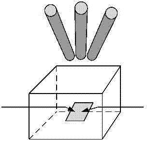
[0009] exist figure 1 Among them, EMMI (1) is non-destructive and fast and precise, and it uses a photon detector to detect the region where the photoelectric effect occurs. Due to the damaged sites on the silicon wafer, there is usually a growing electron-hole recombination resulting in intense photon emission. Therefore, these areas can be detected by EMMI (1); OBIRCH (2) technology is a testing technology that uses laser beams to sense changes in material resistance. Different materials can be scanned by laser beams to measure changes in resistance of different materials; for the same If the material changes due to some factors, the change of resistivity of this material can also be measured. We use this method to detect those hidden dangers in the reliability of metal wiring; SEM (3) is a high-resolution microscopic instrument, which is composed of a scanning system and a signal detection and amplification system. The principle is to use a focused electron beam Bombard t...


PUM


Abstract

The invention provides a multi-channel microscope semiconductor integrated testing system, which is formed by combining an infrared emission microscopy (EMMI) technology, an optical beam induced resistance change (OBIRCH) testing technology, a microprobe detection technology, and a scanning electronic microscopy (SEM) technology. The multi-channel microscope semiconductor integrated testing systemcan effectively perform positioning on defects in a circuit such as holes in a line, holes under a through hole and a high-resistance area at the bottom of a through hole by using an OBIRCH method, and can also effectively detect a short circuit or electric leakage, thereby being a powerful supplement for the emission microscopy technology; and the microprobe detection technology acquires electric parameter values such as operating point voltage, current and a volt-ampere characteristic curve inside an IC quickly and conveniently by a microprobe. The system provided by the invention can perform various failure testing technologies, reduce the test equipment, and is fewer in test step and simple and convenient to operate.

Description

technical field [0001] The invention relates to the field of integrated circuit testing, in particular to a multi-channel microscope semiconductor comprehensive testing system. Background technique [0002] With the development of very large scale integration (VLSI), the feature size of components in semiconductor chips is getting smaller and smaller, and has entered the deep submicron era. The application of integrated circuits is very extensive, and integrated circuits are developing towards smaller process sizes and higher integration levels, and integrated circuit failure analysis is playing an increasingly important role. There can be tens of millions of devices integrated on a single chip, and it is really a needle in a haystack to find a failed device. Therefore, advanced and accurate technology and equipment must be used for integrated circuit failure analysis. Failure analysis is to judge the failure mode, find out the cause of failure, clarify the failure mechanis...

Claims


Application Information

Patent Timeline
IPC IPC(8): G01R31/28G01R31/303G01R31/307G01R31/311
Inventor 陆宇张佩佩程玉华
Owner SHANGHAI RES INST OF MICROELECTRONICS SHRIME PEKING UNIV
Learn More