Method of measuring an alignment mark or an alignment mark assembly, alignment system, and lithographic tool

A technology of aligning marks and alignment systems, which is applied in the photoengraving process, optics, instruments and other directions of the pattern surface, and can solve the problems of sensitivity and so on.

Pending Publication Date: 2021-11-09
ASML NETHERLANDS BV
3 Cites 1 Cited by

AI-Extracted Technical Summary

Problems solved by technology

However, a disadvantage of alignment marks with internal structures is that they may be more sensitive to the location...

Method used

[0114] It has been found that by applying a correction for scan offset in a direction that is not parallel (e.g. perpendicular) to the direction in which the position of the alignment mark is determined, the accuracy of determining an alignment mark AL with an internal structure can be significantly Keep improving. For example, the expected position Xex in the x direction based on the measurement of the coarse alignment marks P1, P2...

Abstract

The invention provides a method of measuring an alignment mark or an alignment mark assembly, wherein the alignment mark comprises grid features extending in at least two directions, the method comprising: measuring the alignment mark or alignment mark assembly using an expected location of the alignment mark or alignment mark assembly, determining a first position of the alignment mark or alignment mark assembly in a first direction, determining a second position of the alignment mark or alignment mark assembly in a second direction, wherein the second direction is perpendicular to the first direction, determining a second direction scan offset between the expected location of the alignment mark or alignment mark assembly in the second direction and the determined second position, and correcting the first position on the basis of the second direction scan offset using at least one correction data set to provide a first corrected position.

Application Domain

Photomechanical treatment

Technology Topic

Mesh gridEngineering +3

Image

  • Method of measuring an alignment mark or an alignment mark assembly, alignment system, and lithographic tool
  • Method of measuring an alignment mark or an alignment mark assembly, alignment system, and lithographic tool
  • Method of measuring an alignment mark or an alignment mark assembly, alignment system, and lithographic tool

Examples

  • Experimental program(1)

Example Embodiment

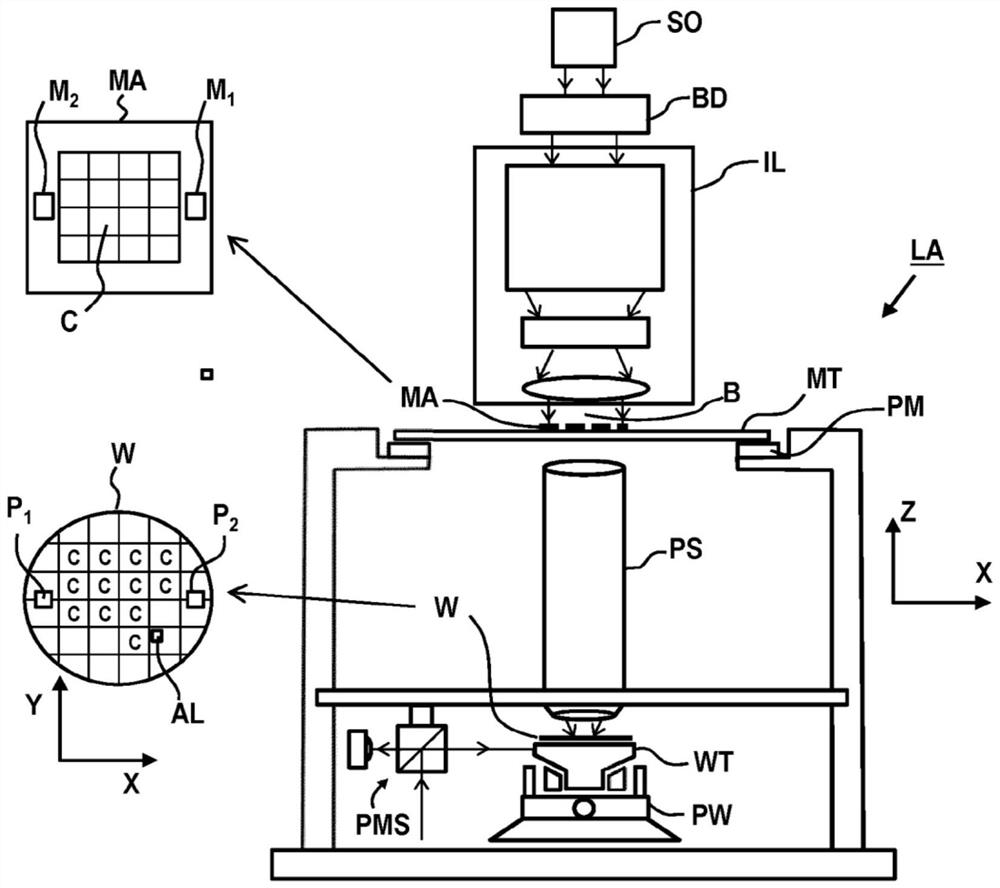
[0067] In this document, the terms "radiation" and "beam" are used to encompass all types of electromagnetic radiation, including ultraviolet radiation (eg wavelengths of 365, 248, 193, 157 or 126 nm) and EUV (extreme ultraviolet radiation, eg wavelengths at in the range of about 5 to 100 nm).
[0068] As used herein, the terms "reticle," "mask," or "patterning device" may be construed broadly to refer to a general-purpose patterning device that can be used to impart a patterned cross-section to an incoming beam of radiation , corresponding to the pattern that will be created in the target portion of the substrate. In this context, the term "light valve" may also be used. In addition to classic masks (transmissive or reflective, binary, phase-shifted, hybrid, etc.), other examples of such patterning devices include programmable mirror arrays and programmable LCD arrays.
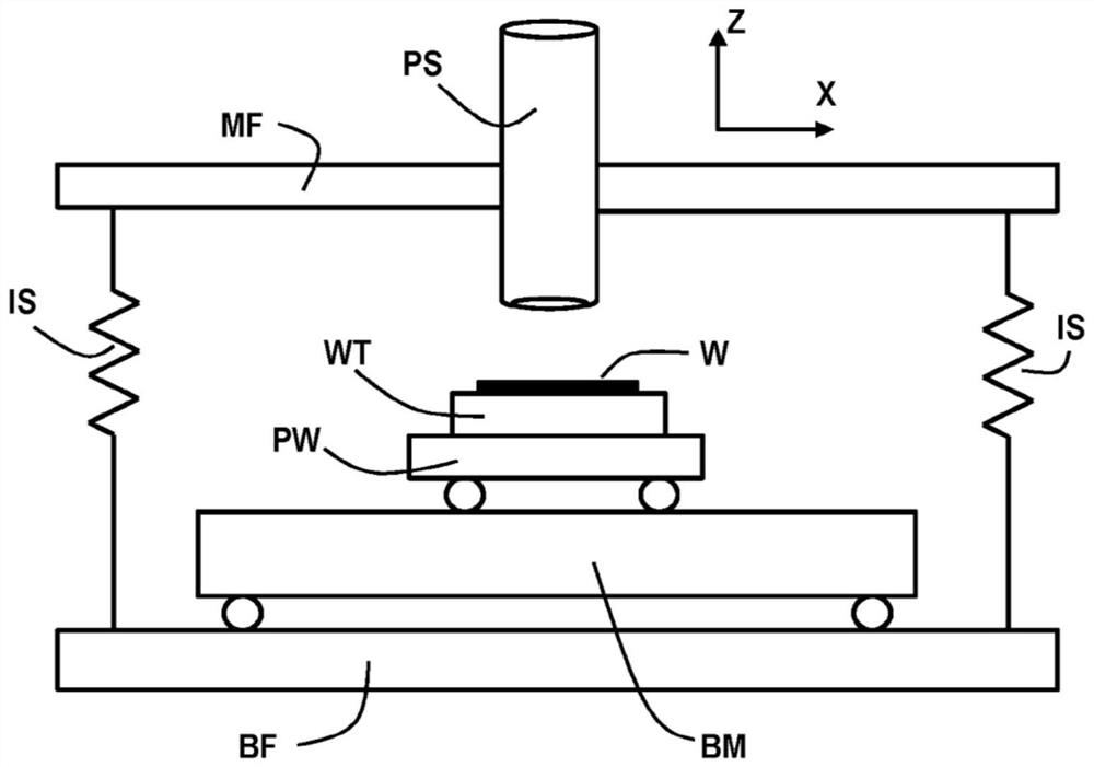
[0069] figure 1 A lithographic apparatus LA is schematically depicted. The lithographic apparatus LA comprises an illumination system (also called illuminator) IL, a mask support (eg mask table) MT configured to condition a radiation beam B (eg UV radiation, DUV radiation or EUV radiation). The mask support MT is configured to support the patterning apparatus (eg mask) MA and is connected to a first positioner PM (configured to accurately position the patterning apparatus MA according to certain parameters), the substrate support (eg a wafer) A stage) WT is configured to hold a substrate (eg, a resist-coated wafer) W and is connected to a second positioner PW (configured to accurately position the substrate support according to certain parameters), and a projection system (eg, a resist-coated wafer) A refractive projection lens system) PS is configured to project a pattern imparted to the radiation beam B onto a target portion C (eg comprising one or more dies) of the substrate W by the patterning apparatus MA.
[0070] In operation, illumination system IL receives a radiation beam from radiation source SO (eg, via beam delivery system BD). The illumination system IL may include various types of optical components, such as refractive, reflective, magnetic, electromagnetic, electrostatic, and/or other types of optical components, or any combination thereof, for directing, shaping, and/or controlling radiation. The illuminator IL may be used to condition the radiation beam B to have a desired spatial and angular intensity distribution in cross-section at the plane of the patterning device MA.
[0071] The term "projection system" PS as used herein should be construed broadly to encompass various types of projection systems, including refractive, reflective, catadioptric, anamorphic, magnetic, electromagnetic and/or electrostatic optical systems or any combination thereof, to suit The exposure radiation used and/or other factors (such as the use of an immersion liquid or the use of a vacuum). Any use of the term "projection lens" herein may be considered synonymous with the more general term "projection system" PS.
[0072] The lithographic apparatus LA may be of the type in which at least a portion of the substrate may be covered by a liquid having a relatively high refractive index, such as water, to fill the space between the projection system PS and the substrate W, which is also referred to as Immersion Lithography. More information on immersion techniques is given in US6952253, which is incorporated herein by reference.
[0073] The lithographic apparatus LA may also be of the type having two or more substrate supports WT (also referred to as "dual stage"). In such a "multi-stage" machine, substrate supports WT may be used in parallel, and/or the step of preparing a substrate W for subsequent exposure may A substrate W is performed while another substrate W on other substrate supports WT is used to expose patterns on other substrates W.
[0074] In addition to the substrate support WT, the lithographic apparatus LA may comprise a measurement stage. The measurement table is arranged to hold the sensors and/or clean the equipment. The sensors may be arranged to measure properties of the projection system PS or properties of the radiation beam B. The measurement table can hold multiple sensors. The cleaning apparatus may be arranged to clean part of the lithographic apparatus, eg part of the projection system PS or part of the system providing the immersion liquid. When the substrate support WT is away from the projection system PS, the measurement table can move under the projection system PS.
[0075] In operation, the radiation beam B is incident on a patterning device (eg mask MA), which is held on the mask support MT, and is patterned by the pattern (design layout) present on the patterning device MA . After traversing the patterning apparatus MA, the radiation beam B passes through a projection system PS, which focuses the beam onto a target portion C of the substrate W. By means of the second positioner PW and the position measurement system PMS, the substrate support WT can be moved accurately, eg in order to position the different target parts C at the focused and aligned positions in the path of the radiation beam B. Similarly, the first locator PM and possibly another position sensor (at figure 1 not explicitly depicted in ) can be used to accurately position the patterning device MA relative to the path of the radiation beam B. Patterning apparatus MA and substrate W may be aligned using mask alignment marks M1, M2 and substrate alignment marks P1, P2. Although the illustrated substrate alignment marks P1, P2 occupy dedicated target portions, they may be located in the spaces between the target portions. The substrate alignment marks P1, P2 may be used as coarse alignment marks, ie alignment marks used to determine the expected locations of other parts of the substrate, such as the expected locations of (fine) alignment marks. Further, the fine alignment marks AL may be provided to determine the location of specific locations of the substrate, whereby the expected locations of the fine alignment marks AL determined by the measurement of the coarse alignment marks P1, P2 are used as the fine alignment marks Basis of measurement for AL.
[0076] To illustrate the present invention, a Cartesian coordinate system is used. A Cartesian coordinate system has three axes, namely, an x-axis, a y-axis, and a z-axis. Each of the three axes is orthogonal to the other two. Rotation around the x-axis is called Rx rotation. Rotation about the y-axis is called Ry rotation. Rotation around the z-axis is called Rz rotation. The x and y axes define the horizontal plane, while the z axis is in the vertical direction. The Cartesian coordinate system does not limit the invention and is used for illustration only. Instead, another coordinate system, such as a cylindrical coordinate system, may be used to illustrate the invention. The orientation of the Cartesian coordinate system can be different, eg so that the z-axis has a component along the horizontal plane.
[0077] figure 2 show figure 1 A more detailed view of a portion of the lithographic apparatus LA. The lithographic apparatus LA may be provided with a base frame BF, a counterweight BM, a metrology frame MF and a vibration isolation system IS. The metrology frame MF supports the projection system PS. Additionally, the metrology frame MF can support a part of the position measuring system PMS. The metrology frame MF is supported by the base frame BF via the vibration isolation system IS. The vibration isolation system IS is arranged to prevent or reduce the transmission of vibrations from the base frame BF to the metering frame MF.
[0078] The second positioner PW is arranged to accelerate the substrate support WT by providing a driving force between the substrate support WT and the balance mass BM. The driving force accelerates the substrate support WT in the desired direction. Due to the conservation of momentum, the driving force is also applied to the counterweight BM with the same magnitude, but in the opposite direction from the desired direction. Typically, the mass of the counterweight BM is significantly greater than the mass of the moving part of the second positioner PW and the substrate support WT.
[0079] In an embodiment, the second positioner PW is supported by a counterweight BM. For example, where the second positioner PW includes a planar motor to float the substrate support WT above the balance mass BM. In another embodiment, the second positioner PW is supported by the base frame BF. For example, wherein the second positioner PW includes a linear motor, and wherein the second positioner PW includes a bearing, such as a gas bearing, to float the substrate support WT above the pedestal BF.
[0080]The position measurement system PMS may comprise any type of sensor suitable for determining the position of the substrate support WT. The position measurement system PMS may comprise any type of sensor suitable for determining the position of the mask support MT. The sensor may be an optical sensor, such as an interferometer or an encoder. The position measurement system PMS may comprise a combined system of interferometers and encoders. The sensor may be another type of sensor, such as a magnetic sensor, a capacitive sensor or an inductive sensor. The position measurement system PMS can determine the position relative to a reference (eg metrology frame MF or projection system PS). The position measurement system PMS may determine the position of the substrate table WT and/or the mask support MT by measuring the position or by measuring the time derivative of the position, such as velocity or acceleration.
[0081] The position measurement system PMS may comprise an encoder system. Encoder systems are known, for example, from US patent application US2007/0058173A1 filed on September 7, 2006, which is incorporated herein by reference. The encoder system includes the encoder head, light grid and sensor. The encoder system can receive the primary radiation beam and the secondary radiation beam. Both the primary radiation beam and the secondary radiation beam originate from the same radiation beam, ie the original radiation beam. At least one of the primary radiation beam and the secondary radiation beam is created by diffracting the original radiation beam with a grating. If both the primary radiation beam and the secondary radiation beam are created by diffracting the original radiation beam with a grating, the primary radiation beam needs to have a different diffraction order than the secondary radiation beam. The different diffraction orders are, for example, the +1st order, the -1st order, the +2nd order and the -2nd order. The encoder system optically combines the primary radiation beam and the secondary radiation beam into a combined radiation beam. Sensors in the encoder head determine the phase or phase difference of the combined radiation beam. Sensors generate signals based on phase or phase difference. This signal represents the position of the encoder head relative to the grating. One of the encoder head and the grating may be arranged on the substrate structure WT. The other of the encoder head and the light grid can be arranged on the metrology frame MF or the base frame BF. For example, a plurality of encoder heads are arranged on the metrology frame MF, and a grating is arranged on the top surface of the substrate support WT. In another example, the grating is arranged on the bottom surface of the substrate support WT and the encoder head is arranged below the substrate support WT.
[0082] The position measurement system PMS may comprise an interferometer system. Interferometer systems are known, for example, from US Pat. No. 6,020,964, filed July 13, 1998, which is incorporated herein by reference. The interferometer system may include beam splitters, mirrors, reference mirrors and sensors. The radiation beam is split by a beam splitter into a reference beam and a measurement beam. The measurement beam travels to the mirror and is reflected back to the beam splitter by the mirror. The reference beam propagates to the reference mirror and is reflected back to the beam splitter by the reference mirror. At the beam splitter, the measurement beam and the reference beam are combined into a combined radiation beam. The combined radiation beam is incident on the sensor. The sensor determines the phase or frequency of the combined radiation beam. Sensors generate signals based on phase or frequency. This signal represents the displacement of the mirror. In an embodiment, the mirror is connected to the substrate support WT. The reference mirror can be connected to the metrology frame MF. In an embodiment, the measurement beam and the reference beam are combined into a combined radiation beam by additional optics rather than a beam splitter.
[0083] The first positioner PM may include a long stroke module and a short stroke module. The short stroke module is arranged to move the mask support MT with high accuracy relative to the long stroke module within a small movement range. The long-stroke module is arranged to move the short-stroke module relative to the projection system PS with relatively low accuracy over a large movement range. With the combination of the long stroke module and the short stroke module, the first positioner PM is able to move the mask support MT relative to the projection system PS with high accuracy over a large movement range. Similarly, the second positioner PM may include a long stroke module and a short stroke module. The short stroke module is arranged to move the substrate support WT with high accuracy relative to the long stroke module within a small movement range. The long-stroke module is arranged to move the short-stroke module relative to the projection system PS with relatively low accuracy over a large movement range. With the combination of the long-stroke module and the short-stroke module, the second positioner PM is able to move the substrate support WT relative to the projection system PS with high accuracy over a large movement range.
[0084] The first positioner PM and the second positioner PW are respectively provided with actuators to move the mask support MT and the substrate support WT, respectively. The actuators may be linear actuators to provide driving force along a single axis (eg, the y-axis). Multiple linear actuators can be used to provide driving force along multiple axes. The actuators may be planar actuators to provide driving force along multiple axes. For example, a planar actuator may be arranged to move the substrate support WT in 6 degrees of freedom. The actuator may be an electromagnetic actuator comprising at least one coil and at least one magnet. The actuator is arranged to move the at least one coil relative to the at least one magnet by applying a current to the at least one coil. The actuators may be moving magnet type actuators having at least one magnet respectively coupled to the substrate supports WT (mask supports MT). The actuators may be moving coil type actuators having at least one coil respectively coupled to the substrate support WT (mask support MT). The actuators may be voice coil actuators, reluctance actuators, Lorentz actuators or piezoelectric actuators or any other suitable actuator.
[0085] The lithography apparatus LA includes image 3 Position control system PCS schematically depicted in . The position control system PCS includes a set point generator SP, a feedforward controller FF and a feedback controller FB. The position control system PCS provides drive signals to the actuator ACT. The actuator ACT may be the actuator of the first positioner PM or the second positioner PW. The actuator ACT drives the device P, which may comprise a substrate support WT or a mask support MT. The output of device P is a positional quantity such as position or velocity or acceleration. The position quantity is measured using the position measurement system PMS. The position measurement system PMS generates a signal, which is a position signal representing the position quantity of the device P. The set point generator SP generates a signal which is a reference signal representing the desired amount of position of the device P. For example, the reference signal represents the desired trajectory of the substrate support WT. The difference between the reference signal and the position signal forms the input of the feedback controller FB. Based on the input, the feedback controller FB provides at least a portion of the drive signal to the actuator ACT. The reference signal may form the input of the feedforward controller FF. Based on the input, the feedforward controller FF provides at least a portion of the drive signal to the actuator ACT. Feedforward FF can utilize information about the dynamic characteristics of the device P, such as mass, stiffness, resonant modes and eigenfrequencies.
[0086] figure 1 The first embodiment of the alignment mark AL is depicted in Figure 4 shown in more detail. The alignment mark AL is a phase grating with a 2x2 sub-grating array AL,a, AL,b, AL,c and AL,d, where the first two sub-gratings AL,a and AL,c are used for alignment in the x-direction, And the last two sub-gratings AL,b and AL,d are used for alignment in the y direction. The first two sub-gratings AL,b and AL,c may have a first grating period, wherein the last two sub-gratings AL,a and AL,d may have a second grating period different from the first grating period.
[0087] The substrate may be provided with coarse alignment marks P1, P2 to measure the positions of the alignment marks P1, P2. This position of the coarse alignment marks P1, P2 can be used to determine the expected location on the substrate where the alignment marks AL are located. In some embodiments, this step in which the coarse alignment marks P1, P2 are used to determine the expected locations of the other alignment marks is designated as Coarse Wafer Alignment (COWA). In a next step, the alignment marks AL and other alignment marks can be measured by the alignment sensor system AS, whereby the expected locations of the alignment marks AL determined based on the coarse alignment marks P1, P2 are used as the scanning alignment marks AL The basics. In some embodiments, this step is indicated as fine wafer alignment (FIWA).
[0088] The position of the substrate alignment mark AL can be measured using an alignment system with an alignment sensor system AS, such as Figure 5 shown. The alignment sensor system AS includes a light source LS that emits light L1 towards the alignment mark AL. The reflected light L2 is diffracted due to the grating of the alignment mark. Diffraction patterns in reflected light are measured using an appropriate detector DE. The positions of the alignment marks can be derived from the diffraction pattern by the processing unit PU.
[0089] The alignment sensor system AS may be provided with multiple light sources, which may share a common processing unit PU. Multiple light sources are advantageous because the signal intensity of monochromatic light reflected from the phase grating varies periodically with the depth of the grating grooves. When using a single-color alignment sensor, the processing of the wafer can affect the depth of the grooves, which in some cases can cause the grating marks to be undetectable or provide a weak signal in others. By providing multiple light sources that each emit light at separate wavelengths, the chance that at least one of the measurement wavelengths provides sufficient signal strength that can be used for alignment position determination is improved. The alignment system may for example use two or four measurement wavelengths, all sharing the same processing unit which processes the signals from the respective detectors. However, other numbers of measurement wavelengths are also contemplated. Note also that in practice the use of multiple measurement wavelengths can be implemented in different ways. Multiple individual sensors can be provided. Also, a single broadband light source can be used.
[0090] because Figure 4 Differences of sub-gratings in alignment marks AL shown, which are alignment marks whose internal structure has sub-regions with distinct grid line features extending in at least two directions, i.e., front The two sub-gratings AL,a and AL,c have grid line characteristics different from those of the latter two sub-gratings AL,b and AL,d. In the embodiment shown, the grid line features of the first two sub-gratings AL,a and AL,c are provided to determine the position in the x-direction, while the grid line features of the last two sub-gratings AL,b and AL,d are provided by Provided to determine the position in the y direction. The grid line features of the first two sub-gratings AL,a and AL,c and the last two sub-gratings AL,b and AL,d comprise grid lines arranged at a certain distance with respect to each other. The spacing of the grating lines of the first two sub-gratings AL,a and AL,c may be the same or different from the spacing of the grating lines of the last two sub-gratings AL,b and AL,d.
[0091] The disadvantage of such an internal structure with different sub-regions is that the internal structure may introduce errors in the measurement due to scan offsets during the scanning of the alignment marks AL. For example, a scan offset in the y direction relative to the center of the alignment mark AL in the y direction may cause measurement errors in the x position of the alignment mark AL. Similarly, a scan offset in the x-direction relative to the center of the alignment mark AL in the x-direction may cause measurement errors in the y-position of the alignment mark AL.
[0092] Similar disadvantages may arise in the measurement of alignment marks, which are relatively small in lateral dimension relative to the measurement beam L1 of the alignment sensor system AS. For example, small alignment marks or alignment mark assemblies may be desirable for in-field alignment marks or alignment mark assemblies to minimize the amount of time required to place the alignment marks or alignment mark assemblies on the substrate space. In such an embodiment, a scan offset in the y-direction and/or the x-direction may cause part of the measurement beam L1 to scan the surrounding structure of the alignment mark rather than the alignment mark itself, which may degrade the position of the alignment mark measurement accuracy. The size of the portion of the measurement beam L1 that will measure the surrounding structure will also depend on the magnitude of the scan offset of the measurement beam L1 in the y- and/or x-direction relative to the centerline of the corresponding alignment mark.
[0093] Furthermore, the intensity distribution of the measurement beam L1 can have an effect on the measurement accuracy depending on the scan offset in the y-direction and/or the x-direction. The intensity distribution depends, for example, on the shape of the cross-section of the measuring beam L1 and/or the homogeneity of the measuring beam L1 over its cross-section.
[0094]A method is proposed to correct the scanning offset of the measuring beam L1 in the second direction by using at least one correction data set, for example by using a correction map calibrated for different scanning offsets of the measuring beam L1 in the second direction. The error in the first direction caused by the displacement. In alternative embodiments, other sets of correction data may be used to correct errors in the positions determined in the first direction based on the determined positions in the second direction, eg defining the scan by the measuring beam L1 in the second direction The relationship between the errors in the first direction due to the offset. These other correction data may include functional relationships, such as functional relationships fitted on experimental data, look-up tables possibly combined with interpolation calculations, and the like.
[0095] The method includes the steps of measuring the alignment mark AL based on the expected location of the alignment mark AL, determining a first position of the alignment mark in a first direction and determining a second position of the alignment mark in a second direction. Subsequently, a scan offset in the second direction between the intended location of the alignment mark AL in the second direction and the determined second position is determined. Finally, the first position is corrected based on the second direction scan offset using the at least one correction data set to provide the first corrected position. The second position may also be corrected based on the determined first direction scan offset between the expected location of the alignment mark AL in the first direction and the determined first position, if desired, using at least one correction data set , to provide the second correction position. Figure 5 The alignment system shown is arranged to perform the method.
[0096] Image 6 shown in more detail for Figure 4 The steps of the method for aligning marks AL are shown. In order to determine the correction position of the alignment mark AL in the x direction and the correction position of the alignment mark AL in the y direction, Image 6 The upper line of shows steps Ax, Bx, Cx, Dx, and Image 6 The lower row shows the steps Ay, By, Cy, Dy.
[0097] As indicated above, based on the measurements of the coarse alignment marks P1, P2, the expected position Xex of the alignment mark AL in the x direction and the expected position Yex of the alignment mark in the y direction can be calculated.
[0098] The expected x position Xex and expected y position Yex of the alignment mark AL define the expected location of the alignment mark AL, which is used as a guide for scanning the measuring beam L1 over the alignment mark AL in the x and y directions, respectively. starting point.
[0099] In step Ax, the alignment mark AL is measured by the alignment sensor system AS by scanning the measurement beam L1 in a measurement scan in the x-direction above the alignment mark AL. Based on the measurement results of this measurement scan in the x-direction, the uncorrected x-position Xnc of the alignment mark AL can be calculated by the processing unit PU, as indicated by the second step Bx. In a third step Cx, the x-direction scan offset OFFx of the measurement scan in the x-direction is calculated by the processing unit PU based on the difference between the expected x position Xex and the calculated uncorrected position Xnc.
[0100] In step Ay, the alignment mark AL is measured by the alignment sensor system AS by scanning the measurement beam L1 in a measurement scan in the y direction above the alignment mark AL. Based on the measurement results of this measurement scan in the y-direction, the uncorrected position Ync of the alignment mark AL can be calculated by the processing unit PU, as indicated by the second step By. In a third step Cy, the y-direction scan offset OFFy of the measurement scan in the y-direction is calculated by the processing unit PU based on the difference between the expected y-position Yex and the calculated uncorrected position Ync.
[0101] In the fourth step Dx, the x-correction map is used to correct the uncorrected x-position Xnc in the x-direction based on the y-direction scan offset OFFy calculated in the step Cy. The x-correction map includes the relationship between the y-direction scan offset OFFy and the calculated corrected APDx for the uncorrected position Xnc. Therefore, in step Dx, the uncorrected position Xnc is corrected using the x-correction map to determine the corrected position Xcor (not mentioned in the drawing), whereby the correction is based on the y-direction scan offset OFFy calculated in step Cy.
[0102] Correspondingly, in the fourth step Dy of calculating the corrected y position Ycor in the y direction, the y correction map is used to correct the uncorrected y position Ync based on the x direction scan offset OFFx calculated in step Cx. The y-correction map includes the relationship between the x-direction scan offset OFFx and the calculated corrected APDy for the uncorrected y-position Ync.
[0103] In practice, both measurement steps Ax and Ay may be performed before any of the calculation steps Bx, Cx, Dx, By, Cy and Dy are performed. It is also possible to perform the calculation steps Bx and Cx before or during the measurement step Ay, or the calculation steps By and Cy before or during the measurement step Ax. Step Dx can only be executed after calculation step Cy is completed, and step Dy can only be executed after calculation step Cx is completed.
[0104] In this application, the term uncorrected position is used to denote a position where the correction described in this application has not (yet) been applied, while a corrected position indicates a position where the correction has been applied. Other corrections not specifically described in this application may be applied to both uncorrected and corrected positions.
[0105] The measured corrected position Xcor of the alignment mark AL in the x-direction can be described by the following equation:
[0106] Xcor=Xnc+APDx(OFFy), where:
[0107] Xcor is the corrected x position,
[0108] Xnc is the uncorrected position of the alignment mark AL based on the expected location of the alignment mark AL in the x-direction based on the alignment mark AL determined with the measurement scan of the alignment mark AL, and APDx(OFFy) is the all measured scan based on the y-direction Correction of the position of the calculated scan offset in the x-direction of the alignment mark AL.
[0109] The measured corrected position Ycor of the alignment mark AL in the y direction can be described by the following equation:
[0110] Ycor=Ync+APDy(OFFx), where:
[0111] Ycor is the corrected y position,
[0112] Ync is the uncorrected position in the y-direction of the alignment mark AL based on the expected location of the alignment mark AL based on the measurement scan of the alignment mark AL, and
[0113] APDy(OFFx) is the correction of the position in the y-direction of the alignment mark AL based on the calculated scan offset of the measurement scan in the x-direction.
[0114] It has been found that the accuracy of determining alignment marks AL with internal structures can be significantly improved by applying a correction for scan offset in a direction that is not parallel (eg perpendicular) to the direction in which the positions of the alignment marks are determined. For example, the expected position Xex in the x-direction based on the measurements of the coarse alignment marks P1, P2 may have an accuracy of +/-200nm, the uncorrected position Xnc in the x-direction obtained by measuring the alignment marks may have +/-200nm 1nm accuracy. By applying a correction map to correct for errors caused by scan offsets in the y direction between the measured scans based on the expected y position Yex and the uncorrected y position Ync, the accuracy of the alignment mark's corrected position Xcor may be improved to +/-0.1nm.
[0115] In some embodiments, the computational accuracy of the positions of the alignment marks AL in the x and y directions can be further improved by applying a further iterative step, where the corrected position Xcor in the x direction is for the scan offset in the y direction is further corrected, and wherein the corrected position Ycor in the y-direction is further corrected for the scan offset in the x-direction. Applying these further iterative steps does not require new measurement scans. An example of n iterations of correcting positions Xcor and Ycor according to these embodiments may be:
[0116] OFFx(n iterations)=Xex-Xcor(n-1 iterations)
[0117] Ycor(n iterations)=Ync+APDy(OFFx(n iterations))
[0118] OFFy(n iterations)=Yex-Ycor(n-1 iterations)
[0119] Xcor(n iterations)=Xnc+APDy(OFFy(n iterations))
[0120] where n is greater than or equal to 2.
[0121] Figure 7 The steps for creating an x-correction map APDx(OFFy) are schematically shown. Multiple scans in the x-direction with different scan offsets in the y-direction are performed with the alignment sensor system AS, and the resulting measurement data are collected. Based on the collected measurement data, the relationship between the correction value APDx and the scan offset OFFy in the y direction can be fitted. Correspondingly, multiple scans in the y-direction with different scan offsets in the x-direction are performed with the alignment sensor system AS, and the resulting measurement data are collected. Based on such collected measurement data, the relationship between the correction value APDy and the scan offset OFFx in the x-direction can be fitted.
[0122] In an embodiment, such calibration of the x-correction map and the y-correction map should advantageously be performed for each alignment mark that requires correction based on scan offset in a non-parallel direction (eg, a direction perpendicular to the measurement direction). For example, in order to use the calibration map, the location of the alignment marks of at least one target portion of the first substrate of the first batch of new layers should be calibrated. In practice, multiple alignment marks of the same layer and possibly from different batches are expected to be calibrated to determine an appropriate correction dataset.
[0123] Figure 8 The alignment mark assembly ALA is shown including a first one-way alignment mark ALX for measuring the alignment position in the x-direction and a second one-way alignment mark ALY for measuring the alignment position in the y-direction . Unidirectional alignment marks are alignment marks with grid features, such as grid lines, that extend in one direction to enable position measurements in a single direction.
[0124] The first alignment mark ALX and the second alignment mark ALY are relatively small compared to the spot size of the measurement beam L1 of the alignment sensor system AS. Therefore, when a measurement scan is performed on the first alignment mark ALX and/or the second alignment mark ALY, a substantial portion of the measurement beam L1 will be scanned on the surrounding structure SUR. Such relatively small alignment marks may also be referred to as overfilled alignment marks compared to the spot size of the measurement beam of the alignment sensor system.
[0125] Scanning of the SUR of surrounding structures may have an effect on the measurement results. The effect will also depend on the scan offset of the measurement beam L1 in a direction perpendicular to the scan direction of the measurement scan relative to the centerline of the alignment mark in this direction. For example, in the measurement scan SCX of the first alignment mark ALX, the measurement scan SCX may have a scan offset in the y-direction with respect to the centerline CEX of the first alignment mark ALX. Similarly, in the measurement scan SCY of the second alignment mark ALY, the measurement scan SCY may have a scan offset in the x-direction with respect to the centerline CEY of the second alignment mark ALY. This scan offset in the x-direction and scan offset in the y-direction typically results from the expected locations of the first alignment mark ALX and the second alignment mark ALY determined based on the rough alignment marks P1, P2, because the rough alignment The marks P1, P2 can only provide the intended locations of the first alignment mark ALX and the second alignment mark ALY.
[0126]Since the first alignment mark ALX and the second alignment mark ALX are relatively close to each other, the scan offset in the x-direction measured with the first alignment mark ALX can be advantageously used to correct for errors in the second alignment mark ALY The scan measurement SCY, and the scan offset in the y-direction measured with the second alignment mark ALY can advantageously be used to correct the scan measurement SCX in the first alignment mark ALX.
[0127] When calculating the positions of the alignment marks ALX and ALY of the alignment mark assembly ALA, the Image 6 and 7 The same correction method explained can be applied. When the effect of the scan offset in the y direction on the position measurement of the first alignment mark ALX in the x direction is known, eg by calibrating and fitting in the first correction map, the scan offset in the y direction The effect of can be corrected by applying a correction based on the uncorrected x position calculated from the measured scan SCX. As explained above, this correction will be based on the y-direction scan offset determined between the expected position in the y-direction and the calculated uncorrected position in the y-direction. Similarly, when the effect of the scan offset in the x-direction on the calculation of the position of the second alignment mark ALY in the y-direction is known, eg by calibrating and fitting in the second correction map, the y-direction The effect of scan offset can be corrected by applying a correction based on the uncorrected y position calculated from the measured scan SCY. The correction will be based on the x-direction scan offset determined between the expected position in the x-direction and the calculated uncorrected position in the x-direction.
[0128] Application of the corrections based on the first and second correction maps will provide a corrected x position of the first alignment mark ALX and a corrected y position of the second alignment mark ALY. This can significantly improve the accuracy with which the positions of the overfilled first and second alignment marks ALX and ALY can be determined.
[0129] Figure 9 Another fine alignment mark ALXY is disclosed that can be advantageously used in methods according to embodiments of the present invention.
[0130] The alignment mark ALXY includes grid lines extending in the x direction to determine the position of the alignment mark ALXY in the y direction and grid lines extending in the y direction to determine the position of the alignment mark ALXY in the x direction.
[0131] The alignment marks ALXY are thin alignment marks suitable for scanning in oblique scan directions, ie scan directions with a non-zero component in the x-direction and a non-zero component in the y-direction. The scanning direction may be, for example, a direction that is 45 degrees from the x-direction and 45 degrees from the y-direction. In this scan direction, the spacing of the grid lines in the x direction should be different from the spacing of the grid lines in the y direction. In alternative embodiments, the scan direction may be at an angle other than 45 degrees relative to the x and y directions. In that case, the spacing of the grid lines in the x direction and the spacing of the grid lines in the y direction may be the same.
[0132] By performing the measurement scan SCXY, sufficient information can be obtained to determine the uncorrected x position of the alignment mark ALXY in the x direction and the uncorrected y position of the alignment mark ALXY in the y direction. The measurement scan SCXY is based on the expected location of the alignment mark ALXY. The expected location includes an expected position in the x-direction and an expected position in the y-direction. The expected location of the alignment marks ALXY can be determined by measuring the positions of the coarse alignment marks P1, P2 of the substrate and estimating the positions of the alignment marks ALXY based on the determined locations of the coarse alignment marks P1, P2.
[0133] exist Figure 9 In the embodiment shown, the spot size of the measuring beam L1 is relatively large compared to the size of the alignment mark ALXY. Therefore, the measurement using the measurement beam L1 may be affected by the surrounding structure SUR of the alignment mark ALXY. The effect of the surrounding structure SUR will also depend on the scan offset in the x-direction and y between the expected scan path based on the actual location of the alignment mark ALXY and the actual scan path of the measured scan SCXY based on the expected location of the alignment mark ALXY Scan offset in direction. According to the method of the present invention, scan offset-related effects of the surrounding structure SUR can be corrected by using a correction map.
[0134] Figure 10 A two-dimensional correction map is shown that can be used to correct scan offsets in the x- and/or y-directions of the measurement scan SCXY to more accurately calculate the y- and x-direction positions of the alignment marks ALXY, respectively.
[0135] Figure 10 The two-dimensional correction map shown was created by aligning with high accuracy to the alignment marks ALXY at defined scan offsets in the x and y directions. The 2D correction map can then be populated by comparing the selected scan offset with the high precision alignment results. Figure 10 The 2D correction map for includes five scan offset locations in the x and y directions, which results in twenty-five scan offset locations. For each of these two-dimensional scan offset locations, a correction value may be determined. The correction value for each scan offset location may eg be based on multiple measurements, eg ten measurements per scan offset location.
[0136] A two-dimensional correction map can be created, for example, for each location of the alignment mark ALXY within the field or target portion, and possibly for each location of the alignment mark ALXY on the complete substrate.
[0137] In an alternative embodiment, by comparing the expected location of the rough alignment and the uncorrected location calculated based on the measured scan SCXY of the alignment mark ALXY with the overlay results for locations at or near the alignment mark ALXY, the correction map can be create.
[0138] When a two-dimensional correction map is available, the uncorrected x-position and uncorrected y-position calculated based on the measurement scan SCXY can be corrected by applying the two-dimensional correction map. Based on the expected position in the x-direction and the calculated uncorrected x-position, a scan offset in the x-direction can be calculated. Correspondingly, based on the expected position in the y direction and the calculated rough y position, the scan offset in the y direction can be calculated. This scan offset in the x direction and the scan offset in the y direction are used to use Figure 10 The 2D calibration plot shown is used to determine the calibration. By applying the correction on the uncorrected x position and the uncorrected y position, the corrected x position and the corrected y position can be calculated separately. It will be clear to those skilled in the art that the scan offset in the x-direction and the scan offset in the y-direction between the expected scan path based on the actual location of the alignment mark and the actual scan path based on the measurement scan of the expected location of the alignment mark This corrected x-position and corrected y-position take into account the influence of the surrounding structural SUR.
[0139] In the above, a method was proposed to improve the accuracy in determining the position of the fine alignment marks. The method may advantageously be used to measure fine alignment marks that are sensitive to scan offsets between a desired scan path based on the actual position of the alignment mark and an actual scan path based on the expected location of the alignment mark.
[0140] Although specific reference may be made herein to the use of a lithographic apparatus in the manufacture of ICs, it should be understood that the lithographic apparatus described herein may have other applications. Possible other applications include the fabrication of integrated optical systems, guidance and detection patterns for magnetic domain memory, flat panel displays, liquid crystal displays (LCDs), thin film magnetic heads, and more.
[0141] Although embodiments of the invention may be specifically mentioned herein in the context of a lithographic apparatus, embodiments of the invention may be used in other apparatuses. Embodiments of the invention may form part of a mask inspection apparatus, metrology apparatus, or any apparatus that measures or processes objects such as wafers (or other substrates) or masks (or other patterning equipment). These apparatuses, such as lithographic apparatuses or metrology apparatuses, may generally be referred to as lithographic tools. Such lithography tools can use vacuum conditions or ambient (non-vacuum) conditions.
[0142] Although the use of embodiments of the invention may have been specifically mentioned above in the context of optical lithography, it is to be understood that the invention is not limited to optical lithography and may be used in other applications where the context permits , such as imprint lithography.
[0143] Where the context permits, embodiments of the present invention may be implemented in hardware, firmware, software, or any combination thereof. Embodiments of the invention can also be implemented as instructions stored on a machine-readable medium, which can be read and executed by one or more processors. A machine-readable medium may include any mechanism for storing or transmitting information in a form readable by a machine (eg, a computing device). For example, machine-readable media may include read only memory (ROM); random access memory (RAM); magnetic storage media; optical storage media; flash memory devices; signal, digital signal, etc.) and others. Further, firmware, software, routines, instructions may be described herein as performing certain actions. It should be understood, however, that this description is for convenience only and that such actions are in fact caused by a computing device, processor, controller or other device executing firmware, software, routines, instructions, etc., and such Doing may cause actuators or other devices to interact with the physical world.
[0144] While specific embodiments of the invention have been described above, it is to be understood that the invention may be practiced otherwise than as described. The above description is intended to be illustrative, not restrictive. Accordingly, it will be apparent to those skilled in the art that modifications of the described invention may be made without departing from the scope of the claims set forth below.

PUM

no PUM

Description & Claims & Application Information

We can also present the details of the Description, Claims and Application information to help users get a comprehensive understanding of the technical details of the patent, such as background art, summary of invention, brief description of drawings, description of embodiments, and other original content. On the other hand, users can also determine the specific scope of protection of the technology through the list of claims; as well as understand the changes in the life cycle of the technology with the presentation of the patent timeline. Login to view more.
Why Eureka
Try Eureka