Method of manufacturing semiconductor device and method of manufacturing power conversion device
A technology of a power conversion device and a manufacturing method, which is applied in the manufacture of semiconductor/solid-state devices, semiconductor devices, circuits, etc., can solve the problems of temperature rise of semiconductor elements and degradation of semiconductor element characteristics.
- Summary
- Abstract
- Description
- Claims
- Application Information
AI Technical Summary
Problems solved by technology
Method used
Image

Examples
no. 1 Embodiment approach
[0044] Next, the semiconductor device and the method of manufacturing the semiconductor device according to the present embodiment will be described. For convenience of description, first, techniques related to the structure of a semiconductor device known to the inventors will be described.
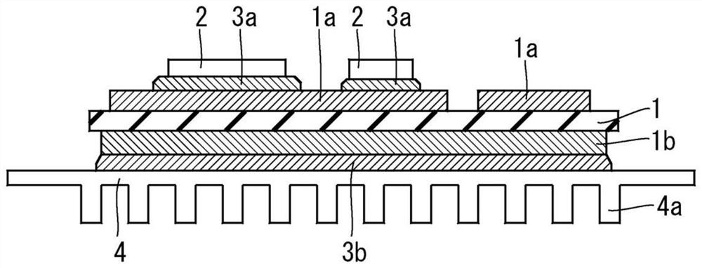
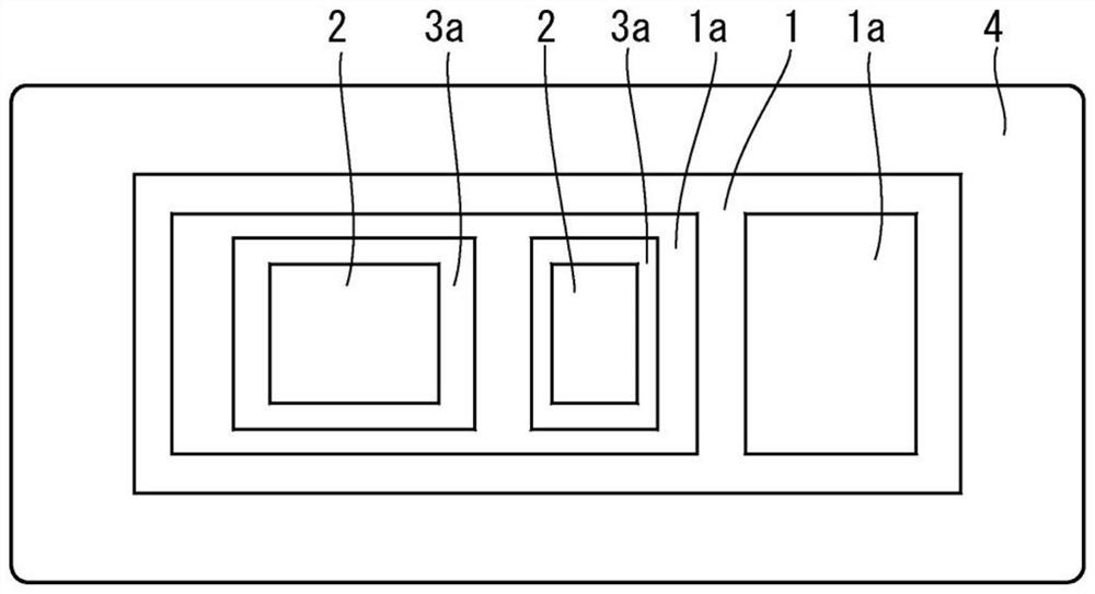
[0045] Figure 16 It is a cross-sectional view schematically showing an example of the structure of a semiconductor device known to the inventor. Such as Figure 16 As illustrated, the semiconductor device has an insulating substrate 1, a plurality of upper surface metal patterns 1a formed on the upper surface of the insulating substrate 1, usually a single lower surface metal pattern 1b formed on the lower surface of the insulating substrate 1, and The semiconductor element 2 is bonded to the upper surface of the upper surface metal pattern 1a via a bonding material 3a such as solder.
[0046] The lower surface metal pattern 1b is bonded to the upper surface of the base plate 4 with ...
no. 2 Embodiment approach
[0079] The semiconductor device and the method of manufacturing the semiconductor device according to the present embodiment will be described. In addition, in the following description, the same structural elements as those described in the above-mentioned embodiment are attached with the same reference numerals and shown in figures, and the detailed description thereof is appropriately omitted.
[0080]
[0081] Figure 10 It is a cross-sectional view schematically showing an example of the structure of the semiconductor device according to this embodiment. Figure 11 yes means Figure 10 A plan view of an example of the structure of the thermally conductive jig 5A illustrated in .
[0082] Such as Figure 10 As illustrated, the semiconductor device has an insulating substrate 1, a plurality of upper surface metal patterns 1a formed on the upper surface of the insulating substrate 1, a lower surface metal pattern 1b formed on the lower surface of the insulating substrat...
no. 3 Embodiment approach
[0088] The semiconductor device and the method of manufacturing the semiconductor device according to the present embodiment will be described. In addition, in the following description, the same structural elements as those described in the above-mentioned embodiment are attached with the same reference numerals and shown in figures, and the detailed description thereof is appropriately omitted.
[0089]
[0090] Figure 13 It is a cross-sectional view schematically showing an example of the structure of the semiconductor device according to this embodiment. Figure 14 yes means Figure 13 A plan view of an example of the structure of the thermally conductive jig 5B illustrated in .
[0091] Such as Figure 13 As illustrated, the semiconductor device has an insulating substrate 1, a plurality of upper surface metal patterns 1a formed on the upper surface of the insulating substrate 1, a lower surface metal pattern 1b formed on the lower surface of the insulating substrat...
PUM
 Abstract
Description
Claims
Application Information
 - R&D
- Intellectual Property
- Life Sciences
- Materials
- Tech Scout
- Unparalleled Data Quality
- Higher Quality Content
- 60% Fewer Hallucinations
Browse by: Latest US Patents, China's latest patents, Technical Efficacy Thesaurus, Application Domain, Technology Topic, Popular Technical Reports.
© 2025 PatSnap. All rights reserved.Legal|Privacy policy|Modern Slavery Act Transparency Statement|Sitemap|About US| Contact US: help@patsnap.com