Supercharge Your Innovation With Domain-Expert AI Agents!

Third-generation semiconductor structure and manufacturing method thereof

A manufacturing method and semiconductor technology, which are applied in semiconductor/solid-state device manufacturing, semiconductor devices, electrical components, etc., can solve the problems of inability to adjust and the ratio of amplified power is small, and achieve the effect of improving the ratio of amplified power and high electron mobility.

Pending Publication Date: 2021-11-19
GALLIUM ADVANCE SEMICON TECH CO
View PDF0 Cites 0 Cited by
  • Summary
  • Abstract
  • Description
  • Claims
  • Application Information

AI Technical Summary

Problems solved by technology

[0005] The main purpose of the present invention is to provide a third-generation semiconductor structure and its manufacturing method, aiming to solve the technical problem that the amplification power ratio is still small and cannot be adjusted

Method used


Image

  • Third-generation semiconductor structure and manufacturing method thereof
  • Third-generation semiconductor structure and manufacturing method thereof
  • Third-generation semiconductor structure and manufacturing method thereof

Examples


Embodiment Construction

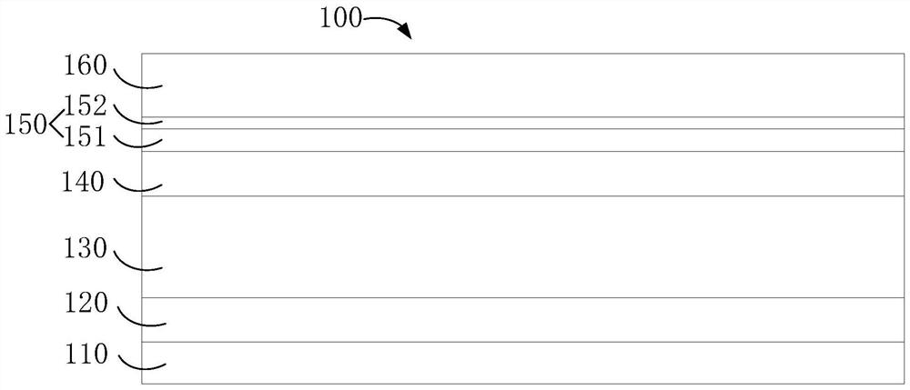
[0039] In order to facilitate the understanding of the present invention, the present invention will be described in more detail below in conjunction with the accompanying drawings and specific embodiments. It should be noted that when an element is said to be "fixed" to another element, it may be directly on the other element, or there may be one or more intervening elements therebetween. When an element is referred to as being "connected to" another element, it can be directly connected to the other element or one or more intervening elements may be present therebetween. The terms "vertical", "horizontal", "left", "right", "inner", "outer" and similar expressions are used in this specification for the purpose of description only. In the description of the present invention, the terms "first" and "second" are used for descriptive purposes only, and cannot be understood as indicating relative importance, or implicitly indicating the quantity of indicated technical features. T...


PUM

PropertyMeasurementUnit
Thicknessaaaaaaaaaa
Thicknessaaaaaaaaaa
Thicknessaaaaaaaaaa

Abstract

The invention relates to the technical field of semiconductor manufacturing, and discloses a third-generation semiconductor structure and a manufacturing method thereof. The third-generation semiconductor structure comprises: a substrate; a buffer layer arranged on the substrate; a collector electrode layer arranged on the buffer layer; a base electrode layer arranged on the collector electrodelayer; a heteroepitaxial layer arranged on the base electrode layer, wherein the heteroepitaxial layer comprises AlGaN; and a radio electrode layer arranged on the heteroepitaxial layer. According to the invention, a heteroepitaxial layer is arranged between a base electrode layer and a radio electrode layer so as to form a two-dimensional electron gas layer to obtain high electron mobility, so that the amplification power ratio of a third-generation semiconductor structure acting on an amplifier is increased; and by adjusting the concentration ratio of Al atoms to Ga atoms in the heteroepitaxial layer, while the important structure of the two-dimensional electron gas layer is maintained, the purpose of adjusting energy of forbidden band electrons of the third-generation semiconductor structure is achieved.

Description

technical field [0001] The invention relates to the technical field of semiconductor manufacturing, in particular to a third-generation semiconductor structure and a manufacturing method thereof. Background technique [0002] In the semiconductor industry, group IV (eg, silicon) based semiconductor devices and / or germanium based semiconductor devices are commonly used to form semiconductor structures. Specifically, in the semiconductor industry, silicon-based semiconductors containing silicon, silicon-germanium alloys, or silicon-carbon alloys are generally available at low cost. [0003] Due to its wide band gap, high breakdown voltage, high electron saturation drift velocity, excellent electrical and optical properties, and good chemical stability, GaN is favored in high-frequency, high-power, high-temperature electronic devices. [0004] In the prior art, when the formed semiconductor structure is used as an amplifier, the amplification power ratio is still small and can...

Claims


Application Information

Patent Timeline
IPC IPC(8): H01L29/06H01L29/20H01L29/207H01L29/778H01L21/335
CPCH01L29/0603H01L29/0684H01L29/7781H01L29/66462H01L29/2003H01L29/207
Inventor 陈正培徐文凯
Owner GALLIUM ADVANCE SEMICON TECH CO
Features
  • R&D
  • Intellectual Property
  • Life Sciences
  • Materials
  • Tech Scout
  • Unparalleled Data Quality
  • Higher Quality Content
  • 60% Fewer Hallucinations
Learn More