Supercharge Your Innovation With Domain-Expert AI Agents!

Semiconductor process chamber, semiconductor process equipment and semiconductor process method

A technology of process chamber and process method, which is applied in the field of semiconductor process equipment, can solve problems such as the inability to ensure stable and uniform air flow, irregular flow channels in the internal space, and affect the quality of film formation, so as to improve the effect of pressure control and shorten the film transfer. Time, the effect of improving the film quality

Active Publication Date: 2021-11-30
BEIJING NAURA MICROELECTRONICS EQUIP CO LTD
View PDF8 Cites 4 Cited by
  • Summary
  • Abstract
  • Description
  • Claims
  • Application Information

AI Technical Summary

Problems solved by technology

However, the transfer structure of the large-capacity multi-reaction zone chamber equipment itself leads to the interconnection of each reaction zone, the transmission chamber has a large space and the flow channel in the internal space is irregular, and the airflow cannot be guaranteed to be stable and uniform.
Further lead to unstable pressure control in the process, and ultimately affect the quality of film formation

Method used


Image

  • Semiconductor process chamber, semiconductor process equipment and semiconductor process method
  • Semiconductor process chamber, semiconductor process equipment and semiconductor process method
  • Semiconductor process chamber, semiconductor process equipment and semiconductor process method

Examples


specific Embodiment

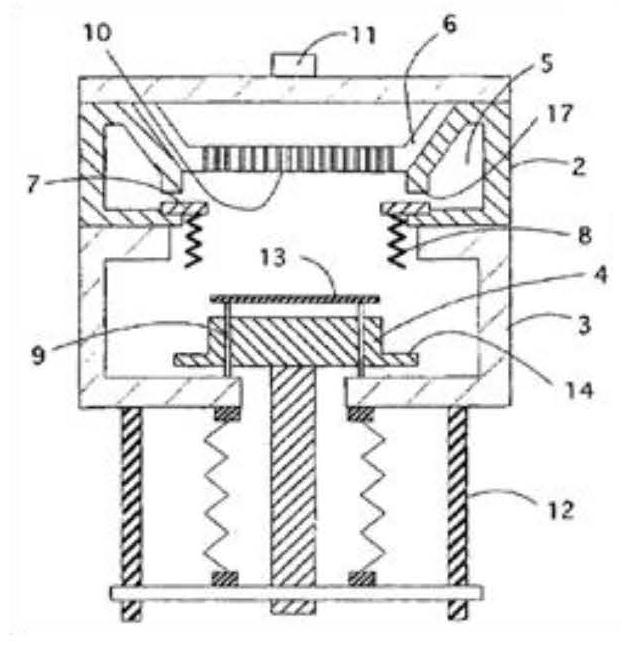
[0102] Before the semiconductor process starts, the four pedestals 300 are all in the low position.

[0103]The wafer 700 is transferred from the outside of the process chamber to the top of the first pedestal 71 and the second pedestal 74 through the transfer port 240, and falls to the plurality of supporting columns 310 corresponding to the first pedestal 71 and the second pedestal 74 respectively. of the upper end. The driving assembly of the transfer manipulator 600 drives the upper flange 62 to rise to a predetermined height and rotate clockwise until the first finger 611 and the second finger 612 respectively rotate under the fourth base 74 and the wafer 700 carried by the first base 71 .

[0104] The driving assembly of the transfer manipulator 600 drives the upper flange 62 to rise again, so that the first finger 611 and the second finger 612 hold up the wafer 700 on the first base 71 and the second base 74 respectively.

[0105] Subsequently, the upper flange 62 is d...


PUM


Abstract

The invention provides a semiconductor process chamber which comprises a reaction cavity and a transmission cavity located below the reaction cavity. The reaction cavity is communicated with the transmission cavity through a bottom opening; a base capable of ascending and descending between the reaction cavity and the transmission cavity is arranged in the semiconductor process chamber; a sealing ring and a first elastic sealing cylinder are further arranged in the semiconductor process chamber; the sealing ring and the first elastic sealing cylinder are both arranged below the base and arranged on a lifting shaft of the base in a sleeving mode; the top end of the first elastic sealing cylinder is in sealing connection with the bottom wall of the sealing ring at an inner hole of the sealing ring; the bottom end of the first elastic sealing cylinder is in sealing connection with the bottom wall of the transmission cavity at a through hole, allowing the lifting shaft to penetrate out, in the bottom of the transmission cavity; and when the first elastic sealing cylinder on the base can ascend to the reaction cavity, the sealing ring is driven to ascend through elastic force and seals the bottom opening of the reaction cavity. According to the semiconductor process chamber provided by the invention, the pressure control effect of the reaction cavity can be improved, the process effect of the semiconductor process is improved, the wafer transfer time is shortened, and the film forming efficiency of the semiconductor process is improved. The invention also provides semiconductor process equipment and a semiconductor process method.

Description

technical field [0001] The present invention relates to the field of semiconductor process equipment, in particular to a semiconductor process chamber, a semiconductor process equipment including the semiconductor process chamber, and a semiconductor process method applied to the semiconductor process equipment. Background technique [0002] With the popularization and upgrading of electronic products and the promotion of the international situation, the semiconductor industry has developed rapidly, and the progress of VLSI is particularly prominent. Each foundry is in urgent need of an optimal expansion plan, that is, to maximize the ratio of production capacity to floor area. At present, there are two main solutions to increase production capacity: 1. Increase the film formation rate, that is, increase the number of film-forming substrates per unit time; 2. Increase the number of film-forming substrates at the same time. [0003] However, using the existing single-wafer p...

Claims


Application Information

Patent Timeline
Patent Type & Authority Applications(China)
IPC IPC(8): C23C16/44C23C16/455H01L21/67
CPCC23C16/44C23C16/45544H01L21/67011Y02P70/50C23C16/4401C23C16/4409H01L21/67126H01L21/68742H01L21/68792H01L21/6719H01L21/68771
Inventor 王勇飞佘清兰云峰
Owner BEIJING NAURA MICROELECTRONICS EQUIP CO LTD
Features
  • R&D
  • Intellectual Property
  • Life Sciences
  • Materials
  • Tech Scout
  • Unparalleled Data Quality
  • Higher Quality Content
  • 60% Fewer Hallucinations
Learn More