
Method for expanding chip selection number and enhancing read-write response time flexibility of SPI (Serial Peripheral Interface)
A technology of response time and chip expansion, applied in the direction of electrical digital data processing, digital memory information, static memory, etc., can solve problems such as timing errors, no response time, SPI can not achieve normal communication, etc., to increase the number of chip selection, increase Response time, port saving effect
- Summary
- Abstract
- Description
- Claims
- Application Information
AI Technical Summary
Problems solved by technology
Method used
Image


Examples
no. 1 example
[0072] For read operations, the following steps are included:
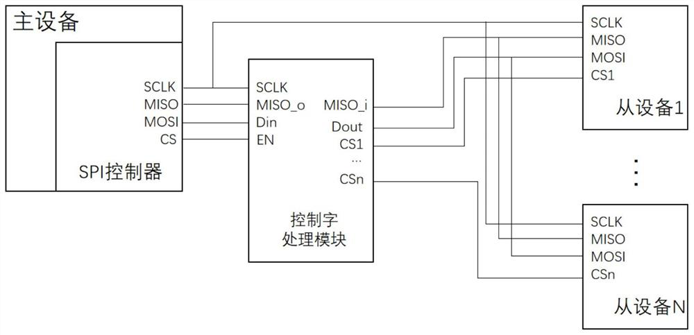
[0073] 1. The SPI controller in the master device sends the control signal to the Din port of the control word processing module via the MOSI port. The chip select port occupied by the existing SPI controller can be simplified as an enable signal port of a control word processing module. If the master device is connected to 8 slave devices, then after applying this scheme, the master device chip occupied by the system The optional port is reduced from 8 to 1, which greatly saves the pins of the chip.
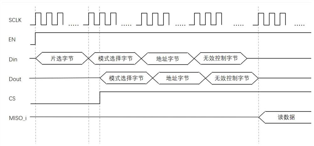
[0074] 2. If the number of slave devices is less than 256, the chip select byte length can be set to 1Byte. Taking the slave device SPI flash chip M25P64 as an example, the format of the control word containing chip selection information is as follows: figure 2 . The control signal includes 1Byte chip selection byte, 1Byte mode selection byte, 3Byte address byte and 1Byte invalid control byte.
[0075] 3. ima...
PUM
 Abstract
Description
Claims
Application Information