Wafer processing method
A processing method and wafer technology, which can be applied to film/sheet adhesives, electrical components, electrical solid devices, etc., can solve problems such as residual quality and reduction, and achieve the effect of improving quality
- Summary
- Abstract
- Description
- Claims
- Application Information
AI Technical Summary
Problems solved by technology
Method used
Image


Examples
Embodiment Construction
[0021] Hereinafter, embodiments of the wafer processing method according to the present invention will be described in detail with reference to the drawings.
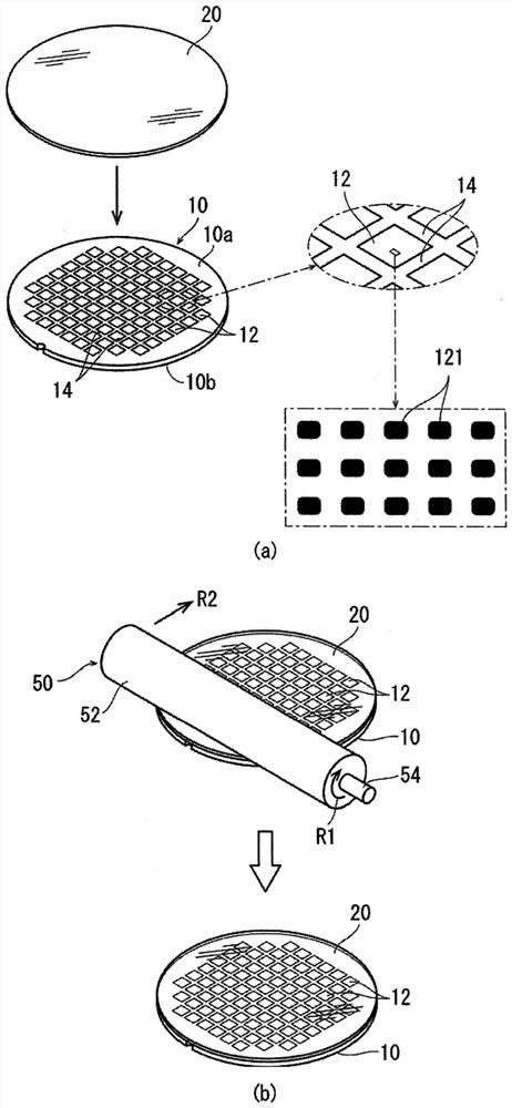
[0022] figure 1 The wafer 10 processed by the wafer processing method of this embodiment is shown in , and an embodiment of the thermocompression bonding sheet disposing process of disposing the thermocompression bonding sheet 20 on the front surface 10 a of the wafer 10 is shown. figure 1 The illustrated wafer 10 is a wafer in which a plurality of electron beam patterning devices 12 are formed on a front surface 10 a divided by dividing lines 14 . The wafer 10 is formed with a thickness of about 150 μm, for example, and the electron beam drawing device 12 is formed in a size of about 3 cm square, for example, as shown enlarged on the right side, and a part of the electron beam drawing device 12 is further enlarged and shown below. As described above, the device is a device in which a plurality of pores 121 with a si...
PUM
 Abstract
Description
Claims
Application Information
 - R&D
- Intellectual Property
- Life Sciences
- Materials
- Tech Scout
- Unparalleled Data Quality
- Higher Quality Content
- 60% Fewer Hallucinations
Browse by: Latest US Patents, China's latest patents, Technical Efficacy Thesaurus, Application Domain, Technology Topic, Popular Technical Reports.
© 2025 PatSnap. All rights reserved.Legal|Privacy policy|Modern Slavery Act Transparency Statement|Sitemap|About US| Contact US: help@patsnap.com