
Photoresist uniform applying device for integrated circuit chip in solar cell panel

A solar panel and integrated circuit technology, applied in the field of solar energy, can solve the problems of uneven flow of glue, increase intelligence, and the inability to change the amount of glue, so as to achieve the effect of uniform glue application, increase intelligence, and reduce waste

Pending Publication Date: 2021-12-03
朱心思
View PDF0 Cites 2 Cited by
  • Summary
  • Abstract
  • Description
  • Claims
  • Application Information

AI Technical Summary

Problems solved by technology

[0003] In the process of applying photoresist to the wafer in the existing integrated circuit chip manufacturing lithography processing system, most of them adopt the method of dispensing glue, but the glue liquid flows unevenly after dispensing, which leads to Uneven wafer gluing will have a negative impact on the quality of subsequent chip production, and when gluing in this way, it is difficult to control the amount of glue falling, which is easy to cause waste of glue, which does not meet the values ​​of energy conservation and environmental protection
[0004] Aiming at the deficiencies of the prior art, the present invention provides a photoresist uniform coating device for integrated circuit chips in solar panels, which has the advantages of changing the amount of gluing and uniform gluing, and solves the problem of existing wafer gluing. The problem of unchangeable glue volume and uneven glue application ensures that when using this device for glue application, it can rotate evenly and apply glue more evenly, and the glue quantity can be adjusted according to the size of the wafer to reduce the waste of glue solution. Increase the intelligence when using the device

Method used


Image

  • Photoresist uniform applying device for integrated circuit chip in solar cell panel
  • Photoresist uniform applying device for integrated circuit chip in solar cell panel
  • Photoresist uniform applying device for integrated circuit chip in solar cell panel

Examples


Embodiment 1

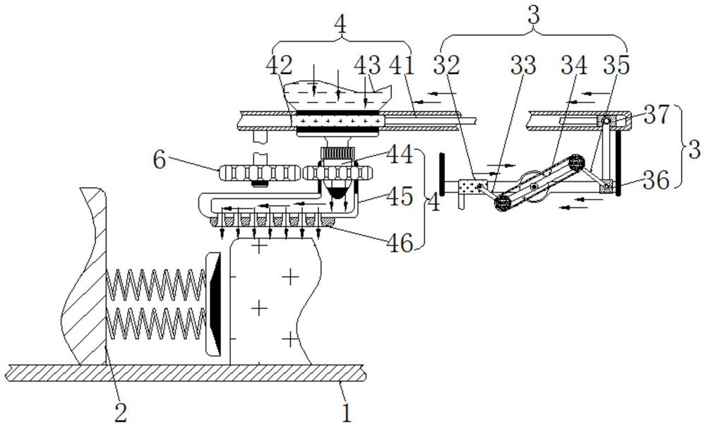
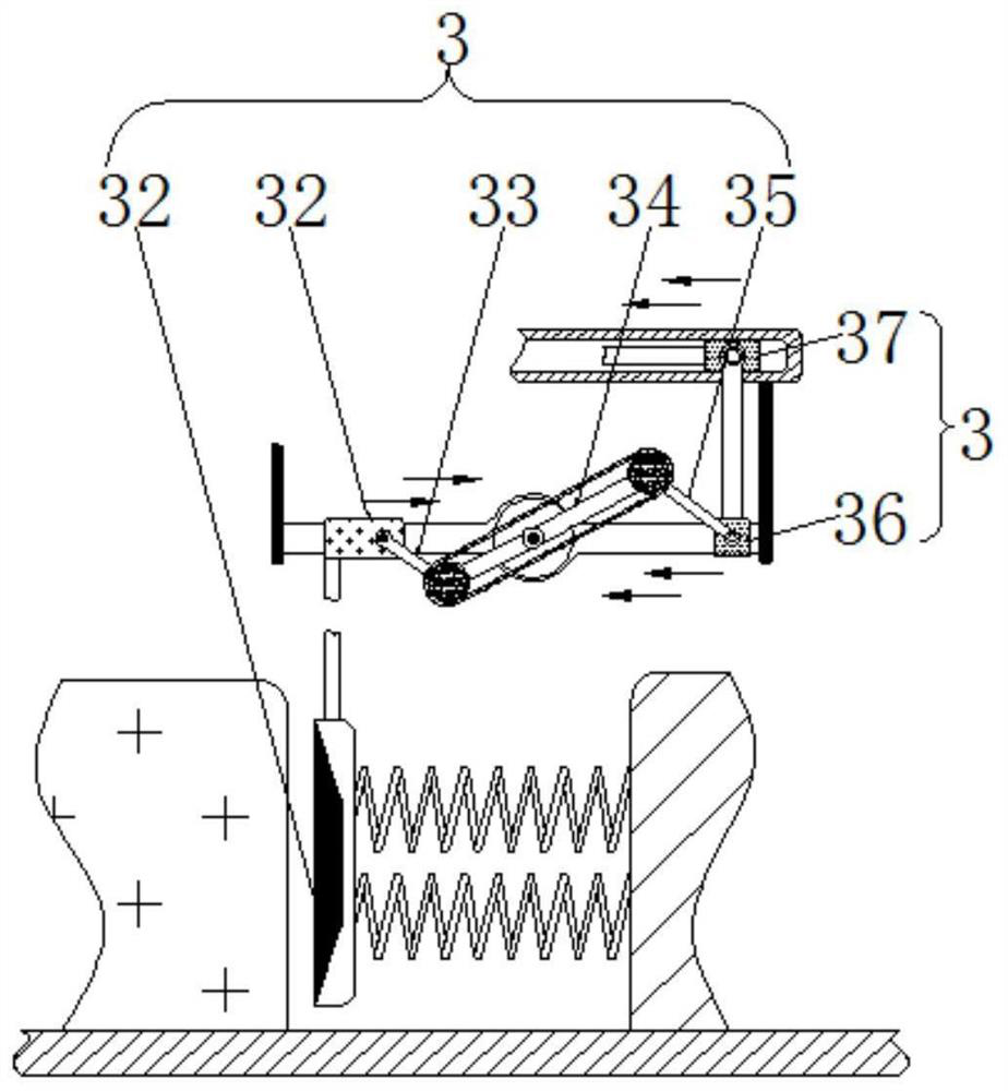
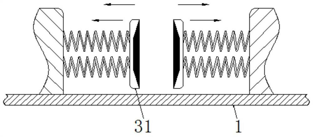
[0023] see Figure 1-2 , a photoresist uniform coating device for an integrated circuit chip in a solar panel, comprising a limit mechanism 3, the limit mechanism 3 includes a limit plate 31, two limit plates 31 are provided, two limit plates 31 The specifications are the same, and they are distributed symmetrically with reference to the center line of the support plate 1. At the same time, a chute is opened on the surface of the limit plate 31, and a spring is arranged between the limit plate 31 and the fixing seat 2. The position plate 31 automatically clamps and limits the wafers being processed to ensure the stability of the wafer processing. At the same time, the limit plate 31 can simultaneously limit the positions of wafers with different radii, improving the intelligence of the device when it is used. The movement of the limiting plate 31 drives the first set of rods 32 to move synchronously, the first set of rods 32 is socketed above the limiting plate 31, and the sur...

Embodiment 2

[0026] see figure 1 , a photoresist uniform coating device for integrated circuit chips in solar panels, and also includes a control mechanism 4, the left end of the slider 37 is welded with a push plate 41, and the end of the push plate 41 away from the slider 37 is clamped with a stop Plate 42, the size of the baffle 42 and the size of the liquid outlet 44 are adapted to each other, and at the same time, a channel is opened inside the scraper 45, and the opening size of the liquid outlet 44 is changed by the movement of the baffle 42, thereby changing the time of gluing. The amount of glue output can improve the intelligence of the device when applying glue, and reduce the waste of glue. The top of the baffle plate 42 is fixedly connected with a liquid storage tank 43, and the inside of the liquid storage tank 43 is provided with a liquid outlet 44. The liquid outlet The outer surface of 44 is sleeved with a scraper 45, and the bottom of the scraper 45 is provided with a spo...

Embodiment 3

[0029] see Figure 1-4 , a photoresist uniform coating device for an integrated circuit chip in a solar panel, comprising a limit mechanism 3, the limit mechanism 3 includes a limit plate 31, two limit plates 31 are provided, two limit plates 31 The specifications are the same, and they are distributed symmetrically with reference to the center line of the support plate 1. At the same time, a chute is opened on the surface of the limit plate 31, and a spring is arranged between the limit plate 31 and the fixing seat 2. The position plate 31 automatically clamps and limits the wafers being processed to ensure the stability of the wafer processing. At the same time, the limit plate 31 can simultaneously limit the positions of wafers with different radii, improving the intelligence of the device when it is used. The movement of the limiting plate 31 drives the first set of rods 32 to move synchronously, the first set of rods 32 is socketed above the limiting plate 31, and the sur...


PUM


Abstract

The invention relates to the technical field of solar energy, and discloses a photoresist uniform applying device for an integrated circuit chip in a solar cell panel. The photoresist uniform applying device comprises a limiting mechanism, the limiting mechanism comprises limiting plates, and a first sleeve rod sleeves the upper portions of the limiting plates. Through cooperative use of the limiting plates, the first sleeve rod, a first connecting rod, a swing rod and a sliding block, wafers of different sizes can be clamped and limited, when the sizes change, the limiting plates can be triggered to move, and finally the opening range of a liquid outlet is changed, so that the purpose of changing the liquid outlet amount of photoresist liquid is achieved, the intelligence during photoresist applying is improved, and waste of the photoresist liquid is reduced. Through cooperative use of the liquid outlet, a scraping plate, liquid outlet holes, a first gear and a second gear, the second gear rotates to drive the scraping plate to synchronously rotate, so that the photoresist liquid is uniformly discharged along the liquid outlet holes, the photoresist liquid is uniformly applied through rotation of the scraping plate, a traditional photoresist dripping mode is changed, and the photoresist liquid is applied more uniformly.

Description

technical field [0001] The invention relates to the technical field of solar energy, in particular to a photoresist uniform coating device for integrated circuit chips in solar panels. Background technique [0002] A solar panel is a device that directly or indirectly converts solar radiation energy into electrical energy through the photoelectric effect or photochemical effect by absorbing sunlight. Circuits, in which photoresist is usually required to be coated on the surface of the wafer during photolithography operations for the fabrication of integrated circuit chips. [0003] In the process of applying photoresist to the wafer in the existing integrated circuit chip manufacturing lithography processing system, most of them adopt the method of dispensing glue, but the glue liquid flows unevenly after dispensing, which leads to Uneven wafer gluing will have a negative impact on the quality of subsequent chip production, and when gluing in this way, it is difficult to co...

Claims


Application Information

Patent Timeline
Patent Type & Authority Applications(China)
IPC IPC(8): B05C5/02B05C11/02B05C11/10B05C13/02
CPCB05C5/02B05C11/1013B05C11/023B05C13/02
Inventor 朱心思
Owner 朱心思
Features
  • Generate Ideas
  • Intellectual Property
  • Life Sciences
  • Materials
  • Tech Scout
  • Unparalleled Data Quality
  • Higher Quality Content
  • 60% Fewer Hallucinations
Learn More